RAM and MAR
Early research - Memories with separate IO or common IO? - MUX, Program Mode and Run Mode - RAM management - Design of the MAR and RAM modules - Schematic - Notes - Useful links

The main limitation of Ben Eater’s SAP-1 computer was certainly the modest amount of addressable RAM, equal to 16 bytes; it was possible to load a simple counter from 0 to 255 and back, or a small Fibonacci algorithm, but nothing more. This was the primary stimulus for the creation of a more powerful computer.
As the completion of the SAP-1 construction was approaching, I had started researching various blogs and forums to gather ideas on possible improvements and expansions.
Early research
The Reddit channel dedicated to Ben Eater’s projects was fundamental in this journey of mine.
From the first article I had read I had taken these notes:
Addressable memory - so the idea here is to have 16bit’s of addressable memory (about 65KB). This would greatly expand the capabilities compared to the 16 bytes of Ben’s PC. This would affect the following things
Memory Address register - after the expansion of course the MAR would have to be 16 bits wide. Here i was considering using 2 x LS273 8 bit flip-flop along with an AND gate to allow the chip to have Input Enable signal (that would be implemented by AND-ing the CLK with an Input signal, since the chip has no InputEnable and i was unable to find one that is 8 bit wide, has CLR and inputenable and did not want to use LS173 but might reconsider)
This user wanted to make a radical expansion of the computer, going from 16 bytes to 64K; my desire was to grow to 256 bytes (and not complicate my life too much with a 16-bit bus), but some information had nonetheless been very useful for a general understanding of the matter.
To address 64K of memory a 16-bit MAR (Memory Address Register) was needed (2^16 = 64K). Instead of using four 4-bit 74LS173 D-type registers, as in the original SAP-1, it seemed more practical to adopt two 8-bit 74LS273 D-type registers. However, the latter had a disadvantage compared to the 4-bit version: they lacked an Enable input. The computer, instead, required this signal, since the MAR had to load a memory address only when specifically requested, and not at every clock cycle. The SAP-1’s MI (Memory Address Register In) signal served precisely this purpose: it allowed the MAR to store the address present on the bus only when necessary, at the Rising Edge of the clock. Conversely, in the absence of an Enable input, the ‘273 flip-flop would have registered the data at every clock cycle.
In my 256-byte project a 8-bit MAR was sufficient (2^8 = 256), so it was possible to simply use two 4-bit ‘173s continuing to exploit the native Enable signals. For completeness, it should be noted that it would also have been possible to use the ‘273 and an AND gate to build an artificial Enable signal: by connecting the CLK and MI signals to the AND inputs, the output would have driven the CLK input of the FF, which would thus have activated only when both signals, CLK and MI, were simultaneously present.
The ‘273, like the ‘173, has a Clear / Reset input (CLR), which in the MAR is needed to reset the register — or at least I believed it was necessary. The alternative hypothesis of using a 74LS377 8-bit register, which includes 8 FFs with Enable, also seemed interesting; initially I believed it was not possible to proceed in this way, because the MAR also needed the CLR, not present in this chip. Later I had realized that the MAR could work perfectly well without a Clear / Reset signal; the ‘377 would become one of the most widely used chips in the BEAM.
Program counter - would have to be expanded to a 16 bit counter (should be trivial to do that) I currently have tons of 8 bit counters combined with a register (and the 4 bit 161 counters that Ben used)
As in the case of the MAR, to address 256 bytes of RAM an 8-bit Program Counter (PC) register was needed. In the SAP-1 computer a 4-bit counter 74LS161 was present instead and I therefore had to try to combine two of them in cascade.
It would have been convenient to use a single 8-bit counter, but among the chips available on the market I could not find one that also included the LOAD input. The LOAD allows the parallel loading onto the PC of a specific address to which the computer must jump (for example, to execute an absolute jump or relative branch instruction).
To combine two 4-bit chips it was necessary, and also very useful, to understand the difference between “Ripple Mode Carry” and “Carry Look Ahead”: the 74LS161 counter datasheet in fact reported these two different examples of connecting chips in cascade with each other. A deeper discussion on the topic can be found in a dedicated section of the page devoted to Binary Arithmetic.
Instruction register - now sh!t gets fun. Since i want to bomb completely, I am considering having a 3 byte Instruction register in a way mimicking the BIU block & instruction queue in a 8086. The idea here is to split the instruction register in 3 bytes. 1 byte would be for the instruction/opcode alone, the second and third are going to hold the data of the instruction (either address or an immediate value). This would allow you to address the entire memory space. Also instructions can be of different size. For example. OUT (move to out register) would be just 1 byte wide, LDI (load immediate) would be 2 bytes and LDA (load address/absolute) would be 3 bytes wide. The control logic would take care of the fetch cycle. Or in other words since you know the instruction you are execution you would know how much bytes the instruction is and thus fetch either 1, 2 or 3 bytes from the RAM.
After reading this point I had started gathering my thoughts for the 256-byte memory expansion, an idea I return to later in this page. Certainly, I had no intention of building a multi-byte IR, or in any case an IR capable of holding both the opcode and the operand. I imagined first reading the opcode and loading it into the Instruction Register and, subsequently, reading the operand and handling it appropriately.
Memories with separate IO or common IO?
Until now, I had almost substantially taken for granted that I would continue using memory chips with separate Input and Output ports (“dual-port”), exactly as happens in the 74189 used in the SAP. However, in this Reddit post, a user highlighted difficulties in sourcing the 74189 and asked for clarification on the use of the 62256; I thus began to delve deeper into the characteristics of this “single-port” chip, increasing my understanding of these two different architectures.
Originally I had highlighted these few notes present in the post, reflecting on the fact that this user’s approach to managing control signals seemed to me a bit too simplified, but further along in time I had realized that, all things considered, writing to the RAM is not excessively complex:
62256 - The I/O lines are controlled by OE and CE. When either are high puts the I/O lines at high impedance. When both are low, the RAM outputs data onto the I/O lines. Writing takes place (two ways, but this is one way) CE low and OE high. A low pulse on WE will write the data on the I/O lines into the RAM chip.
- CE = Chip Enable
- OE = Output Enable
- WE = Write Enable
The user notes that there are two write modes; the one he highlights requires OE HI, CE LO and the WE LO pulse; the other mode reported in the datasheet (“WE Controlled”) requires both OE and CE at LO state and the WE LO pulse. In this second mode the only signal to manage is WE, which will need to be HI during read phases and pulsed LO during write phases. In the first and second schematic of the RAM module of my own design I had adopted the first of the two modes, while in the final module — and after having better understood the implications of each — I used the second mode. Other notes relating to the topic can be found later on this same page.
Another aspect that I had immediately noticed, hypothesizing the use of the 62256, was the impossibility of maintaining visibility of the content of the RAM cell addressed by the MAR using LEDs (or at least so I believed): if with the ‘189s the output ports were always active and I could see at any moment the value contained in the memory cell currently addressed by the MAR, with the 62256 I would have had visibility of the cell content only at the moment when the RAM was being read — and therefore not continuously.

Schematic of Ben Eater’s RAM module: note the 74189s with dedicated Input ports D1-D4 and dedicated Output ports O1-O4.
What I was beginning to understand was that to use a RAM with Common IO I had to do a “double pass” or something similar. How do I always keep the content of the memory location visible even at the moment when I set the IO ports of the chip to input mode? How do I maintain visibility of the RAM content when it is not active in output? Do I perhaps need to store the content of the RAM outputs in some latch and only at that point disable the chip before writing to it? Later I would understand that a latch was not necessary, but that there was another way.
In this post a user presented a drawing that I believed could work, but in his schematic the multiplexer (MUX) outputs are always active (the multiplexer 74LS157 multiplexers are not tri-state) and could create contention with the RAM outputs when the latter is active in output; the solution could be to add another bus transceiver 74LS245, or to use MUX tri-state 74LS257; I had some intuition regarding the need to manage the RAM control signals in a more comprehensive way and to control the interactions with the MUXes and with the transceiver(s) interfacing with the computer bus.

Paper drawing of the RAM and MAR module to understand the best chip arrangement based on the required connections.
MUX, Program Mode and Run Mode
What are the MUXes for in the RAM module (and in the MAR)? At power-on, the content of the RAM memory is empty / random, so we must first have the possibility to program the RAM (“Program Mode”) and then to make it visible to the computer bus during normal program execution (“Run Mode”).
-
Program Mode is manual and uses dip-switches to manually address and program the RAM.
-
Run Mode is the execution mode, in which the RAM is addressed exclusively by the MAR and is equally accessed for reading / writing only by the computer bus; note that it is possible to manually switch to Program Mode to read or write the RAM content in a “debug mode” style and then resume normal program execution.
The selection of what to pass to RAM and MAR is done through a MUX (in our case 2:1, i.e. each output corresponds to two selectable inputs): the MUX inputs are connected both to the dip-switches we will use for manual programming of the computer and to the computer data bus; the outputs are connected to the RAM and MAR inputs. A simple switch connected to the MUX selection input allows choosing which inputs to activate.
For example, in the SAP-1 schematic visible higher up on this page, the ‘157 multiplexers manage the RAM inputs: the MUX inputs are connected both to the dip-switch and to the computer bus, while the outputs are connected to the D1-D4 input ports of the ‘189 RAM chips.
I returned to the theme of the “double pass” (or better “double bus”, as I would understand later), which from what I was beginning to understand could make possible the persistent display of the RAM content. On pages 17 and 18 of “Building the SAP-3 rev 3.3.pdf” present in the GitHub repository of rolf-electronics, another user of the Reddit channel, I had noticed that a second ‘245 transceiver had been inserted.

The operation and necessity of the transceivers were very clear to me, as they were widely used in the SAP-1 computer to be able to activate the various computer modules only when it was necessary to do so: typically each module needs a single interconnection transceiver toward the bus.
Rolf’s RAM module schematic instead provides two, one “internal” and one “external”, to separate the data path toward the RAM from that of the data from the RAM:
- The left transceiver is active when writing to the RAM, selecting the source via the ‘157 MUX (which in “Program Mode” activates the inputs connected to the dip-switch, while in “Run Mode” activates the inputs connected to the bus); the LEDs show the value being written to the RAM
- The right transceiver is active when reading from the RAM; the LEDs show the value being read from the RAM and transferred to the computer bus.
A latch to store the LED state, as I had initially and incorrectly assumed, was not necessary.
Continuing my research, I had found this schematic by user jaxey1631, who had left a comment in Ben Eater’s video Reprogramming CPU microcode with an Arduino:

RAM and MAR with dual bus.
In this schematic we find:
-
The 62256 RAM chip.
-
A ‘273 FF in the upper right which, lacking an Enable as discussed earlier, activates in correspondence with a fictitious Enable built with the logical operation “Clock AND Memory Address Register In” (inputs 1A and 1B of the NAND on the left in the schematic); the MI signal indicates that the computer is preparing to set the RAM address on which it will perform the next operation.
-
The two ‘157 MUXes at the top that allow the selection of addresses (between those set on the dip-switches or those present on the outputs of the ‘273 FF) to be exported toward the A0-A7 pins of the RAM chip. The selection of the inputs activated by the MUX occurs thanks to the mode selection switch (upper left) connected to the SEL inputs: in Program Mode the red LED is on and the SEL inputs are at LO state, activating the A1-A4 inputs of the MUXes; in Run Mode the green LED is on and the SEL inputs are at HI state, activating the B1-B4 inputs.
-
Another two ‘157 MUXes at the bottom that allow the selection of what to export toward the D0-D7 data pins of the RAM chip; these MUXes are also connected to the mode selection switch and activate the inputs connected to the address selection dip-switch or those connected to the computer bus, depending on the state of the switch (Program Mode or Run Mode).
-
A first ‘245 transceiver (at the bottom) whose inputs are connected to the outputs of the two MUXes mentioned in the previous point. This transceiver acts as an interface toward the RAM (the DIR pin set to LO configures pins A1-A8 as inputs and pins B1-B8 as outputs) and activates at the moment when data must be written to memory; the OE signal of this first transceiver is in fact active when the Write Button is pressed (lower left) in Program Mode, or in correspondence with Clock + RI (RAM In) (see inputs 4A and 4B of the central NAND on the left in the schematic) when in Run Mode;
-
A second ‘245 transceiver that activates at the moment when data must be read from the RAM and its output transferred toward the data bus (in this case too the DIR pin of the ‘245 set to LO configures pins A1-A8 as inputs and pins B1-B8 as outputs); note its OE input connected to the RO (RAM Output) signal of the computer.

62256 “WE Controlled” Write Cycle.
Note the configuration of the RAM chip: the CE and OE signals are always active, which means that the user has decided to use the write mode defined as “WE# Controlled” defined on page 6 of the 62256 datasheet. Re-reading these notes a good while after completing my project, everything seems easy, but understanding the RAM write modes was actually quite a lengthy process.
It is also worth noting that this user too does not use the CLR on the ‘273 FFs of the MAR input — thinking about it, it might really not be needed, because every time I need to access the RAM, I preventively set the desired address on the MAR. The reset at power-on was probably more aesthetic than anything else.
It was at this moment (August 2022) that I discovered the NQSAP, adding it to my notes as “there’s this guyhttps://tomnisbet.github.io/nqsap/docs/ram/ that seems to have made some nice modifications to his computer” 😁; I decided to follow this project because it allowed building an Instruction Set like that of the 6502 which, as I would later discover, would require a large number of addresses for the EEPROM microcode
Among the various links explored for the RAM upgrade, there was also Step-by-Step Guide to Upgrading the RAM with Pictures, which many users found well done, but which I found particularly difficult to digest as it lacked a schematic.
To add a further useful link for understanding RAM module architectures, I highlight this Reddit post. The explanations are very well done and useful. The RAM chip used is interesting because it presents itself as two distinct RAMs, each with dedicated access and a Busy signal to manage parallel requests on the same location. Another noteworthy aspect of this user’s implementation is the possibility of increasing the number of computer instructions up to 256, thanks to the choice of using a full byte for the instruction and an optional subsequent byte for the operand, rather than having a single byte of which the 4 Most Significant Bits (MSB) represent the opcode and the 4 Least Significant Bits (LSB) are the operand, as in Ben Eater’s SAP-1.
A collateral (but very important) aspect of increasing the number of instructions was the need to increase the size of the EEPROMs hosting the microcode: wanting to manage (up to) 256 instructions, 8 instruction bits, 3 step bits and 2 flag bits = 13 total pins were needed, making 28C64s necessary… and I had forgotten that I would need an additional bit for the selection of the two EEPROMs! At that moment, I did not yet know that I would spend entire weeks understanding the fantastic Flag module of Tom Nisbet’s NQSAP, which has a completely different approach and does not require output signals from the EEPROMs.
RAM management
Among the most useful posts relating to the understanding of RAM and MAR management signals for the memory module with common IO, there is certainly the Question about RAM replacement, in which the moderator The8BitEnthusiast invites consulting his (excellent, I would add) implementation, which I took as an example and inspiration.

RAM module by Reddit user and moderator The8BitEnthusiast.
On the one hand, the schematic appeared simplified compared to those I had seen previously; on the other hand, the use of only one ‘157 MUX, with signals going out to re-enter other gates, made it difficult to understand and analyze. I had therefore tried to build myself the timing diagrams of the signal schematics for these three possible cases:
- Writing to the RAM in Run Mode

- Reading from the RAM while in Run Mode

- Writing to the RAM while in Program Mode

The8BitEnthusiast noted that he had exploited the propagation delay of the ‘245s to manage the timing requirements, at which point I had tried to ask him whether it was necessary to manage timings in such a precise way because his project was working in “just in time” mode every time a clock pulse arrived.
For example, I assumed that in the first case “Writing to the RAM while in Run Mode” the following occurred.
-
Before the Rising Edge of CLK:
- we are in Run Mode, therefore PROG is HI
- the MUX enables inputs I1a, I1b, I1c
- Zb is HI (since input I1b is connected to Vcc) and therefore the right ‘245, which connects the programming - dip-switch, is disabled
- the RI signal is HI (RI = RAM In, i.e. writing to the RAM), therefore we are preparing a write
- the /RO signal is HI (RO = RAM Out, i.e. reading from the RAM), therefore reading from the RAM is disabled
- Zc = /(CLK LO * RI HI) = HI, therefore the direction of the left ‘245, which connects the data bus, is A–>B - (Output)
- Za = //(/RO HI * Zc HI) = HI, therefore the ‘245 from/to the data bus is disabled
-
CLK active:
- Zc = /(CLK HI * RI HI) = LO, therefore the direction of the ‘245 from/to the data bus is B–>A (Input)
- Za = //(/RO HI * Zc LO) = LO, therefore the ‘245 from/to the data bus is active
- /WE = Zc = LO, therefore the RAM receives the Falling Edge of the Write signal and finds at its inputs what is projected onto it by the ‘245 from/to the data bus
-
When the clock pulse ends:
- Zc = /(CLK LO * RI HI) = HI, therefore the direction of the ‘245 from/to the data bus is A–>B (Output)
- /WE = Zc = HI, therefore the Write pulse on the RAM ends with the Rising Edge
- Za = //(/RO HI * Zc HI) = HI, therefore the ‘245 from/to the data bus is disabled
Legend:
- PROG is the signal of the Program Mode (LO) / Run Mode (HI) mode selection switch; in the original SAP-1 computer schematics it is found in the MAR
- / means NOT
- * means AND

Writing to the RAM while in Run Mode.
From what I was reading, I imagined that the critical moment was the Rising Edge of the Clock, because at that point it is necessary to wait for the RAM to be ready for writing and it is precisely here that it is necessary to exploit the delay introduced by the ‘245 to show the data to the RAM “a little later”, but I did not understand exactly why.
The8BitEnthusiast had kindly replied to my question:
I had to make sure that the ‘245s did not deliver data to the RAM when it was not yet ready to accept data as Input because its outputs were still active in output**. The datasheet states that the RAM disables the output and is ready for input 20 nanoseconds after WE is brought to LO state.

** In the schematic of The8BitEnthusiast’s RAM module it can be noted that the OE signal of the RAM is connected to ground, which means that the data pins are always active in output, except when a write must be performed. When the write signal WE is activated, there is a time tWHZ during which the RAM is still active in output; once this time has elapsed, it is possible to put data in input on the RAM.
In other words, the RAM is normally active in output; to write to it, it must be activated in input with the WE signal. Since the RAM takes 20 nanoseconds to switch the data pins from output to input, before applying input signals to it it is necessary to wait at least 20 nanoseconds from the moment WE is activated (otherwise short circuits could be caused: for example having an output pin on the RAM at HI and the corresponding input pin on the transceiver at LO would mean bringing the RAM output directly to ground, short-circuiting it).

The8BitEnthusiast continued:
The same Zc signal that activates writing to the RAM (WE) also enables the two ‘245s; the ‘245 datasheet specifies that its activation requires 25 nanoseconds, which is a value greater than that required by the RAM to activate in input, so the requirement is met
In other words, the RAM receives the write signal at the same moment the transceiver receives the enable signal, but the transceiver is slower than the RAM and therefore the RAM pins will already be in the correct input mode before the transceiver outputs what is present at its inputs.
Very, very clever.
Design of the MAR and RAM modules
In parallel with the study of other users’ work, I had started working on the design of my own MAR and RAM modules, while continuing to open other lines of study to deepen partially obscure topics or tackle new subjects. I regularly had dozens of web pages open simultaneously.
The MAR
The MAR was designed at 8 bits to drive 256 memory addresses. Initially I had used two 4-bit ‘173 FFs, later replaced by a single 8-bit ‘273 FF (lacking output activation control, which however is not necessary). Finally I used an 8-bit ‘377 register, equally suited to our purpose.
")
BEAM Memory Address Register (MAR).
Note the Program Mode / Run Mode selection switch (signal /PROG, which is also connected to the RAM module):
- when contacts 1-2 are closed the ‘157 MUX selection pins are at logic state LO, activating inputs I0a, I0b, I0c and I0d, which thus transmit to the RAM address bus the values set on the dip-switch;
- when contacts 2-3 are closed the ‘157 MUX selection pins are at logic state HI, activating inputs I1a, I1b, I1c and I1d, which thus transmit to the RAM address bus the values present at the ‘377 output.
First version of the RAM module
As already mentioned, regarding the construction of the RAM module I had decided to proceed with the 62256 chip with common IO. To try to fix the concepts, I had transcribed again the differences between the architectures with chips with separate IO and common IO:
- With dual-port RAMs, I had the RAM IN and RAM OUT signals on “separate” buses:
- the “IN” bus connected the outputs of the 74LS157 MUXes to the Data In pins of the RAMs: the MUXes were always active on the “Write” ports of the RAMs and showed them everything that was happening on the main computer bus in Run Mode or on the DIP-Switch in Program Mode, but it was not a problem, since the RAMs only wrote in correspondence with the RI (RAM In) signal;
- the “OUT” bus connected the ‘245 transceiver and the Data Out outputs of the RAMs; the transceiver output was enabled only in correspondence with the /RO (RAM Out) signal.
-
With the single-port RAM the Data lines are instead the same for Write and Read. Depending on the operation to be performed, two different paths are activated, as already discussed when talking about the dual bus. To write to the RAM the sequence was as follows:
- Output Enable /OE fixed LO;
- Chip Enable /CE pulsed LO (“↘↗”);
- /WE ↘↗ (which must be “contained” within the ↘↗ cycle of /CE).
 module")
First version of the BEAM memory (RAM) module.
I had high hopes for this first design.
To write to RAM in Run Mode:
- RI (which in the Write cycle is HI) enables the upper ‘245 via a NOT gate;
- /RO (which in the Write cycle is HI) brings /OE to HI, disabling the 62256 output;
- /CE (aka /CS, Chip Select) is fixed LO as it is connected to ground;
- the values present on the bus or on the dip-switch are presented via MUX to the transceiver which, in turn, presents these values to the RAM ports;
- Zd, and therefore /WE, is HI, since pin 1 of the NAND is LO;
- at the Rising Edge of the Clock the NAND output goes from HI to LO for the RC time and the /WE ↘↗ pulse is transmitted to the RAM through the ‘157 MUX: the RAM stores whatever it finds at its D0-D7 input ports.
In Program Mode the I0d input of the MUX is HI thanks to the 1K pull-up resistor, but by pressing the button a negative pulse is created that activates a /WE ↘↗ cycle: in this case too the RAM stores whatever it finds at its D0-D7 input ports.
To read from the RAM the following conditions must be met:
- /CE LO, i.e. the chip must be enabled
- /OE LO, i.e. the outputs must be activated
- /WE HI, therefore I must not activate the write signal
The sequence of events is therefore as follows:
- RI is LO, therefore the NOT gate will disable the upper transceiver, which will therefore not output anything toward the RAM;
- RO LO enables the lower XCVR and /OE of the RAM, which is activated in output;
- /CE (aka /CS, Chip Select) is fixed LO as it is connected to ground;
- meanwhile WE is HI (and therefore writing is inhibited) because:
- in Run Mode RI LO keeps HI at the output of the NAND connected to I1d of the MUX (if one of the two RAM inputs is LO, the output is HI) and therefore /WE is also fixed HI, inhibiting writing;
- in Program Mode the I0d input of the MUX is fixed HI thanks to the 1K resistor, so in this case too there is no writing.
A subsequent analysis of this schematic, which “to the eye” was very attractive, showed me that I had probably managed the “internal bus” concept correctly and that the output phase could also be functional, while in the input phase I noticed superfluous redundancies: I could have made the lower transceiver work bidirectionally depending on the need to allow RAM and BUS to interact and I could also have eliminated the MUXes and connected the upper transceiver directly to the dip-switch, activating it only at the right moment for manual RAM programming. In practice, I would have returned to the solution conceived by The8BitEnthusiast, without however having yet acquired sufficient capability and autonomy to design a just-in-time transceiver activation solution as he had done
Second version of the RAM module
Having established that a just-in-time solution would have been premature for my skill level, I had therefore tried to redraw the schematic with only one transceiver while keeping the MUXes to manage the RAM input, making it come from the bus or from the dip-switch depending on Program or Run Mode.
 module")
Second version of the BEAM memory (RAM) module.
In terms of timing this is also the official moment of the birth of the name BEAM 😁.
After completing the drawing, it seemed to me that I had added more chips (for the logic) compared to before = greater complexity. However, the idea continued to appeal to me and it was an interesting logical exercise to try to exploit the single transceiver by reversing its direction depending on the operation to be performed.
I had tried to ask for advice on Reddit and the ever-tireless The8BitEnthusiast had given me some guidance and an overall positive response.
To analyze all possible logic states I had prepared a summary table with which to verify whether the module’s behavior was in line with expectations; the table shown below is only a part of the complete one.

Summary table of logic state analysis for the second version of the RAM module.
At a certain point I realized that there was a rather significant problem in the schematic: the two ‘157 MUXes were continuously projecting their inputs toward the internal bus, causing a possible short with the RAM when the latter was in output mode. I therefore thought of replacing the 2x ‘157s with the ‘257s, which are tri-state
Revised summary table of logic state analysis for the second version of the RAM module.
When I reached this point I realized I had been working unnecessarily: what do two MUXes and a ‘245 serve? Two ‘245s are sufficient, one to manage the I/O on the bus and one to manage the dip-switch, which is in fact what The8BitEnthusiast had done! I had been enlightened and at that moment everything seemed clear to me!
In the meantime I had also started renaming the logic signals taking the computer rather than the module as the point of view:
| Old | Description | New | Description |
|---|---|---|---|
| RI | RAM In | WR | Write RAM |
| RO | RAM Out | RR | Read RAM |
and so on.
Third version of the RAM module
I had therefore finally rewritten the “truth table” of the RAM module:

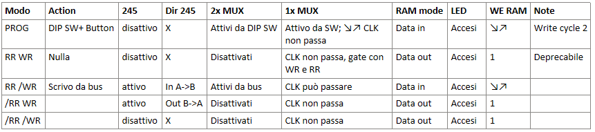
RAM module analysis table - third version.
The two asterisks in the table ** served to remind me that I had to be particularly careful in the preparation of the microcode and that I must never have /WR and /RR active simultaneously, because I had not provided hardware control to prevent a possible conflict (to avoid conflicts I would have had to put a 3-input NAND on /WR that activates only for CLK, RR and /WR, i.e. /WE = CLK * RR * /WR, in other words: I can write to the RAM only if I am not reading from it).
Schematic
 module")
Third version of the BEAM computer memory (RAM) module.
Returning to the 62256 datasheet, on page 6 we find both write modes: the one indicated as “WRITE CYCLE 2 (CE# Controlled)” had been used for the first two revisions of the RAM module; the other, “WRITE CYCLE 1 (WE# Controlled)”, is the one used for the final module design, because keeping /OE and /CE fixed LO for both reads and writes represented an important simplification.

Signal management passes in an important way through the ‘157 MUX, as also happens in The8BitEnthusiast’s schematic, but with some differences.
Here is a summary of the possible states:
- /PROG: In Program Mode the MUX activates inputs I0a, I0b, I0c and I0d. In Run Mode I1a, I1b, I1c and I1d are active.
- Za is normally HI through the resistor connecting it to Vcc, but switches to LO when the programming button is pressed and activates /WE, writing to the RAM.
- Zb is normally HI through the resistor connecting it to Vcc, but switches to LO when the programming button is pressed and activates the transceiver that interconnects the RAM and dip-switch.
- Zc is fixed HI and deactivates the transceiver that interconnects the RAM and bus.
- RR WR: Read RAM and Write RAM are not active.
- Za is fixed HI (because the NAND on I1a has a fixed LO input) and writing to the RAM is inhibited.
- Zb is fixed HI and inhibits the transceiver between the RAM and dip-switch.
- Zc is fixed HI and deactivates the transceiver that interconnects the RAM and bus.
- RR /WR: Read RAM is not active, Write RAM is active.
- Za is normally HI (because the NAND on I1a has a LO input), but at the clock pulse it switches to LO and activates /WE, writing to the RAM.
- Zb is fixed HI and inhibits the transceiver between the RAM and dip-switch.
- Zc is normally HI, therefore deactivates the transceiver that interconnects the RAM and bus, but at the clock pulse it switches to LO (because Za switches to LO), activating the transceiver.
- /RR WR: Read RAM is active, Write RAM is not active.
- Za is fixed HI (because the NAND on I1a has a fixed LO input) and writing to the RAM is inhibited.
- Zb is fixed HI and inhibits the transceiver between the RAM and dip-switch.
- Zc is fixed LO and activates the transceiver between the RAM and bus.
- /RR /WR: Illegal state.
Notes
Instead of the more common dip-switches, I used very convenient Rocker Switches (“a bilanciere”) like those in the figure; they can easily be found at electronics distributors. Note that the original pins are quite short and do not correctly fix the switch to the breadboard, so I added an integrated circuit socket.

Rocker Switch.
Useful Links
- The documentation “Building the SAP-3 rev 3.3.pdf” written by rolf-electronics and available on GitHub.