Binary Arithmetic
Key concepts - Sources - Unsigned and Signed Numbers - Overflow in depth - Overflow and hardware - Overflow identification methods - Simplification with 74LS151 - Addition and subtraction verification with 74LS151 - Adders - Additions with the Adders - Multiple Bit Adder - Ripple Carry Adder - Carry Look Ahead Adder - Implementation in the 74LS181 - Subtractions with the Adders - Useful links
Key concepts
While studying the operation of the Flag and ALU modules, I had discovered several gaps in my binary arithmetic knowledge:
- Unsigned and Signed binary numbers
- Representation methods for signed binary numbers:
- Sign and Magnitude (Signed Magnitude)
- One’s Complement (1C)
- Two’s Complement (2C)
- Addition and subtraction of binary numbers
- Unsigned Overflow and Signed Overflow
Sources
Far from wanting (or being able) to explain everything on this page, I try to summarize what I had learned to remedy my gaps and suggest a series of sources for further study.
For a complete understanding of the topics covered, I recommend accessing the information multiple times, even at different times and in different sequences: with repeated readings and further study I had achieved the set goal, while multiple viewings of the videos in “brainstorming” mode had allowed me to fill the gaps until they were filled.
Here is a series of YouTube videos:
-
Binary Overflow - Mr Powell’s Computer Science Channel - link: generic concept of Overflow.
Let us assume we have an 8-bit computer, capable of adding two 8-bit numbers: both the addends and the sum are 8-bit numbers that can therefore range from 0 to 255.
- Adding for example 73 + 114 gives 187, which is a number representable with 8 bits;
- Adding instead for example 175 + 92 gives 267, which is not representable with an 8-bit number: we have an Overflow error (or unsigned Overflow), because the bits at our disposal (8) do not allow us to represent the result of the sum: the result of the arithmetic operation exceeds the representation capacity of the available bits without considering the sign.
We essentially have a carry that we should bring to the 9th bit of our computer, which however only has 8. In this case the Carry output signal from the ALU signals to us that the number resulting from the sum of the two addends is larger than the number calculable by the ALU.
-
Sums of Unsigned numbers, the concept of Carry and possible Overflow - Mr Dimmick’s Computing Channel - link: very well done; also explains the basic rules applicable to all binary number additions.
-
Negative Numbers in Binary by the same author as video #1 - link: an excellent video that explains how to represent negative numbers in two’s complement and how to convert a positive number to negative and vice versa.
- With two’s complement, there is only one 0, unlike what happens with Sign and Magnitude (see further on in this page).
- To convert a positive number to negative it is sufficient to invert all the bits and add 1.
- The same procedure is perfectly valid in reverse as well (from negative to positive).
- Pay attention to an error also acknowledged by the author in the comments: in the discussion of Sign and Magnitude the range does not go from -64 to +64, but from -128 to +127.
-
Twos complement: Negative numbers in binary by Ben Eater - link: more on negative numbers, complements and subtractions. Excellent for understanding how two’s complement addresses the shortcomings of one’s complement.
-
Binary Addition and Subtraction With Negative Numbers, 2’s Complements & Signed Magnitude - The Organic Chemistry Tutor - link: excellent video with very effective graphical visualization.
-
Particularly interesting is a comment noting that to invert the sign of a binary number represented in 2C it is sufficient to follow two steps: 1) start from the right and do not modify anything up to and including the first bit equal to 1; 2) invert all remaining bits.
Example: to invert the number 01010100 (decimal 84) leave the first 3 bits from the right unchanged (01010100) and then invert all the others from 01010100 to 10101100, obtaining as the final result 10101100 (-84)
-
-
Two’s Complement Arithmetic by Brock LaMeres - link: despite the not-perfect audio quality (but the pronunciation remains excellent and easily understandable even for someone who is not a native speaker), the presentation of the topic is excellent.
And some pages to visit:
- The Overflow (V) Flag Explained by Bruce Clark on 6502.org - essential language and lots of information.
- The 6502 overflow flag explained mathematically by Ken Shirriff - an incredibly well-done page covering Complements, Signed numbers, Overflow.
- The 6502 CPU’s overflow flag explained at the silicon level by Ken Shirriff - very interesting analysis of Overflow at the silicon level of the 6502.
- Signed Binary Addition Calculator - calculator for sums of Signed numbers with highlight of the various calculation steps.
I highlight in particular The 6502 overflow flag explained mathematically for a complete understanding of Overflow, which will be revisited and deepened later in this page.
Unsigned and Signed Numbers
It is necessary to thoroughly understand the logic and differences relating to Unsigned and Signed numbers.
Delving deeper into Signed numbers, I had come across this very interesting page from the University of Mississippi dedicated to binary mathematics.
Thanks to the section Textbook ==> Module 3: Computer Integer Arithmetic ==> 2. Negative binary numbers I had perfectly understood the binary representation of negative numbers.
The Signed Magnitude method is very easy to understand: one bit is sacrificed by dedicating it to the representation of the sign; the sacrificeable bit is the most significant one (MSB), therefore if an 8-bit Unsigned number can go from 0 to 255 (2^8 = 256 representable combinations), an Unsigned number will have 7 bits available for the Magnitude (2^7 = 128 combinations) and one bit for the sign, therefore it can go from -128 to +127 (always 256 representable numbers, but half negative and half positive).
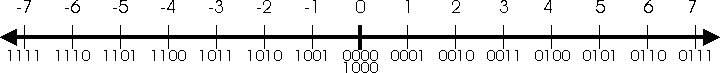
Sign and Magnitude representation of 4-bit numbers.
In the image (simplified to just 4 bits for space reasons) a non-trivial problem can be noted: zero appears twice (0000 and 1000): we know that zero has no sign, therefore this representation is not the best possible.
Note: on the cited page, there is an incorrect image in the subtraction “5 - 2”. The image is as follows:
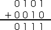
The page actually wanted to represent a subtraction between A and B using the Sign and Magnitude method, which should allow transforming the operation from “5 - 2” to “5 + (-2)” by inverting the first bit of the number 2, which therefore goes from 0010 to 1010
   Dec        Bin
A     5  ==>  0101+
B    -2  ==>  1010
   ----       ----
Q     3       1111 ==> -7
However, the binary sum of 0101 (5) and 1010 (-2) does not lead to the expected result (3), but rather to a clear error: it is clear that the Sign and Magnitude representation does not allow transforming an “A - B” operation into “A + (-B)”.
Setting aside the explanation of the One’s Complement (1C) method (inversion of all bits of the number), which is also not optimal, Two’s Complement (2C) is instead perfect for the representation of negative numbers, also bringing with it a great simplification in the execution of subtractions.

Two’s Complement representation of 4-bit numbers.
Two aspects are worth highlighting:
- Resolution of the double-zero problem.
- The rule underlying the two’s complement theory is: how can I represent the number “-1” so that, by adding “1” to it, one obtains “0”?
- Similarly to old mechanical odometers in cars, which once they reached 99,999 went to 00,000, the 99,999 of the odometer corresponds to the 1111.1111 of 8-bit binary arithmetic: added to 0000.0001, it generates as a result 0000.0000. Note: in this page, the separator point between the first 4 bits and the second 4 bits of 8-bit binary numbers is inserted only to facilitate reading and does not in any way modify their values.
- Subtractions can be performed without errors by adding the minuend and the two’s complement of the subtrahend.
- For example, instead of performing “15 - 7”, one performs “15 + (-7)”: addition is the simplest operation to perform and implement; using two’s complement it becomes possible to apply to subtractions the same rules already applied to additions, enormously simplifying the calculations.
- For further study of subtraction in 2C, see the links previously highlighted, in particular video number #4.
Returning also to what was described on the Flags page, 256 combinations are possible in a byte:
- treating numbers as Unsigned, it is possible to count from 0 to 255;
- treating numbers instead as Signed in two’s complement:
- values from 0 to 127 are represented in the same way as Unsigned numbers from 0 to 127 (from Hex 0x00 to 0x7F);
- values from -128 to -1 are paired with the hexadecimal and binary representations of Unsigned numbers from 128 to 255 (from Hex 0x80 to 0xFF).
This table should clarify the concept:
----------------------------------------
| Hex  | Binary    | Signed | Unsigned |
----------------------------------------
| 0x80 | 1000.0000 |   -128 |      128 |
| 0x81 | 1000.0001 |   -127 |      129 |
| 0x82 | 1000.0010 |   -126 |      130 |
| 0x83 | 1000.0011 |   -125 |      131 |
| .... | ......... |    ... |      ... |
| .... | ......... |    ... |      ... |
| .... | ......... |    ... |      ... |
| 0x90 | 1001.0000 |   -112 |      144 |
| 0xA0 | 1010.0000 |   - 96 |      160 |
| 0xB0 | 1011.0000 |   - 80 |      176 |
| 0xC0 | 1100.0000 |   - 64 |      192 |
| 0xD0 | 1101.0000 |   - 48 |      208 |
| 0xE0 | 1110.0000 |   - 32 |      224 |
| 0xF0 | 1111.0000 |   - 16 |      240 |
| 0xF1 | 1111.0001 |   - 15 |      241 |
| 0xF2 | 1111.0010 |   - 14 |      242 |
| 0xF3 | 1111.0011 |   - 13 |      243 |
| .... | ......... |    ... |      ... |
| .... | ......... |    ... |      ... |
| .... | ......... |    ... |      ... |
| 0xFD | 1111.1101 |   -  3 |      253 |
| 0xFE | 1111.1110 |   -  2 |      254 |
| 0xFF | 1111.1111 |   -  1 |      255 |
----------------------------------------
| Hex  | Binary    | Signed | Unsigned |
----------------------------------------
| 0x00 | 0000.0000 |      0 |        0 |
| 0x01 | 0000.0001 |      1 |        1 |
| 0x02 | 0000.0010 |      2 |        2 |
| 0x03 | 0000.0011 |      3 |        3 |
| .... | ......... |    ... |      ... |
| .... | ......... |    ... |      ... |
| .... | ......... |    ... |      ... |
| 0x10 | 0001.0000 |     16 |       16 |
| 0x20 | 0010.0000 |     32 |       32 |
| 0x30 | 0011.0000 |     48 |       48 |
| 0x40 | 0100.0000 |     64 |       64 |
| 0x50 | 0101.0000 |     80 |       80 |
| 0x60 | 0110.0000 |     96 |       96 |
| 0x70 | 0111.0000 |    112 |      112 |
| 0x71 | 0111.0001 |    113 |      113 |
| 0x72 | 0111.0010 |    114 |      114 |
| 0x73 | 0111.0011 |    115 |      115 |
| .... | ......... |    ... |      ... |
| .... | ......... |    ... |      ... |
| .... | ......... |    ... |      ... |
| 0x7C | 0111.1100 |    124 |      124 |
| 0x7D | 0111.1101 |    125 |      125 |
| 0x7E | 0111.1110 |    126 |      126 |
| 0x7F | 0111.1111 |    127 |      127 |
Relationship between 8-bit Hex, Bin, Signed and Unsigned numbers.
As already seen in the image Two’s Complement representation of 4-bit numbers, it is important to note here as well the transition of Signed numbers from -1 to 0 in correspondence with the binary transition from 1111.1111 to 0000.0000. Two’s complement is, therefore, a very practical way to represent Signed numbers, in which an MSB = 0 indicates a positive number and an MSB = 1 indicates a negative number. The MSB equal to 1 assumes the negative value 2^n, where n is the position of the MSB itself (the position count is performed starting from zero and moving from right to left). In the case of an 8-bit number, the MSB is worth -(2^7) = -128. The sum between the MSB and the values assumed by the other 7 bits corresponds to the value of the number expressed in Signed notation. Let us look at two examples by summing the values of the bits equal to 1::
- 0010.0011 =      0 + 0 + 2^5 + 0 + 0 + 0 + 2^1 + 2^0 =        32 + 2 + 1 =  35
- 1010.0011 = -(2^7) + 0 + 2^5 + 0 + 0 + 0 + 2^1 + 2^0 = -128 + 32 + 2 + 1 = -93
Overflow in depth
An in-depth study of Overflow was a mandatory step; before understanding the operation of the circuit section dedicated to the V flag, I needed a thorough understanding of its definition and of the methods used to determine it.
Tom Nisbet noted that the inspiration for the use of a 74LS151 Data Selector/Multiplexer to identify Overflow situations in his NQSAP derived from a Reddit thread, which then referred to pages written by Dieter Mueller (aka ttlworks) on 6502.org.
In the reference link, Dieter initially explained in a visual manner in which addition or subtraction situations between two 8-bit Signed numbers an Overflow would be generated, using what could perhaps be defined as a sort of Pythagorean table.
Let us recall that Overflow indicates an error in the process of adding or subtracting two Signed numbers: if the resulting number has an incorrect sign compared to what was expected, there is an Overflow.
In the two tables below, which represent addition and subtraction operations respectively, the Column/Row combinations at whose intersection there is an asterisk “*” indicate Overflow situations, i.e. a result that cannot be correctly represented with the 8 available bits.
Operation        Sum  (Column + Row)       Sub (Column - Row)
                   +0123456789ABCDEF         +0123456789ABCDEF
                 +  0000000000000000       -  0000000000000000
Overflow:        00 ................       00 ................
Overflow:        10 .......*........       10 ........*.......
Overflow:        20 ......**........       20 ........**......
Overflow:        30 .....***........       30 ........***.....
Overflow:        40 ....****........       40 ........****....
Overflow:        50 ...*****........       50 ........*****...
Overflow:        60 ..******........       60 ........******..
Overflow:        70 .*******........       70 ........*******.
Overflow:        80 ........********       80 ********........
Overflow:        90 ........*******.       90 .*******........
Overflow:        A0 ........******..       A0 ..******........
Overflow:        B0 ........*****...       B0 ...*****........
Overflow:        C0 ........****....       C0 ....****........
Overflow:        D0 ........***.....       D0 .....***........
Overflow:        E0 ........**......       E0 ......**........
Overflow:        F0 ........*.......       F0 .......*........

Example:        0x70 + 0x40 = Overflow    0xA0 - 0x30 = Overflow
Notes:
- The tables are simplified: only multiples of 16 (0xX0) are shown, therefore 0x00, 0x10, 0x20 and so on.
- 8-bit Signed numbers are represented, therefore, for example, 0x20 corresponds to decimal 32, while 0xA0 corresponds to decimal -96.
- As described in the table Relationship between 8-bit Hex, Bin, Signed and Unsigned numbers, the range of 8-bit Signed numbers extends from -128 (0x80) to 127 (0x7F) passing through zero (0x00).
Let us return to the two Overflow examples shown at the bottom of the tables:
0x70 + 0x40 = in decimal 112 + 64 = 176, which however does not fall within the -128 / +127 range of 8-bit Signed numbers. In fact, the sum of 112 and 64 generates a result whose MSB is 1, which according to Signed notation is a negative number. Since we have added Signed numbers, the result must also be read as Signed: 0xB0 = -80, which is clearly incorrect. From this we derive that if the sum of two positive Signed numbers generates a negative Signed result, we are in an Overflow situation, i.e. a number not representable with the available bits.
  Hex       Dec       Bin
                      1
  0x70 ==>  112  ==>  0111.0000 +
 +0x40 ==>   64  ==>  0100.0000 =
           ----     -----------
            176       1011.0000 ==> 0xB0
0xA0 - 0x30 = -96 - 48 = -144, which however does not fall within the -128 / +127 range of 8-bit Signed numbers. In fact, the subtraction between -96 and 48* generates a result whose MSB is 0, which according to Signed notation is a positive number. Since we have subtracted Signed numbers, the result must also be read as Signed: 0x70 = 112, which is clearly incorrect. From this we derive that if the subtraction between a negative Signed and a positive Signed generates a positive Signed result, we are in an Overflow situation, i.e. a number not representable with the available bits.
  Hex       Dec       Bin
                     1
  0xA0 ==>  -96  ==>  1010.0000 +
 -0x30 ==>  -48  ==>  1101.0000 =
           ----     -----------
           -144      10111.0000** ==> 0111.0000 ==> 0x70
* Note that in this second case the ALU internally performs an A + (-B) operation, therefore the representation of B is inverted according to the two’s complement (2C) rule.
** The 9th bit is truncated, because the size of the word used in the operation is 8 bits.
In addition to the two examples cited just above, it is worth anticipating that the opposite hypotheses are also demonstrable:
- if the sum of two negative Signed numbers generates a positive Signed result, we are in an Overflow situation;
- if the subtraction between a positive Signed and a negative Signed generates a negative Signed result, we are in an Overflow situation.
In conclusion, we can say that if the sign bit is corrupted an Overflow has occurred and the V flag is consequently set.
Overflow and hardware
Dieter presented a logical representation of an Adder capable of performing both additions and subtractions, noting that “additions A+B are easy; to perform subtractions instead, the simplest method is to invert B and then proceed exactly as for additions: A+(-B)”.
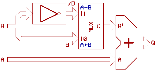
Adder hardware for A+B additions and A-B subtractions.
In an 8-bit Adder we have 8 1-bit Adders in cascade; the one represented below is the 8th and last, whose inputs A and B’ are the most significant bits A7 and B7’ of the numbers to be added; the Carry-in input C_IN is connected to the Carry-Out output C_OUT coming from the previous Adder.
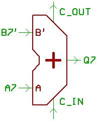
Last stage of an 8-bit Adder.
The following table summarizes what happens in the 8th Adder:
| C7 | B7’ | A7 | Q7 | C8 | V |
|---|---|---|---|---|---|
| 0 | 0 | 0 | 0 | 0 | 0 |
| 0 | 0 | 1 | 1 | 0 | 0 |
| 0 | 1 | 0 | 1 | 0 | 0 |
| 0 | 1 | 1 | 0 | 1 | 1* |
| 1 | 0 | 0 | 1 | 0 | 1** |
| 1 | 0 | 1 | 0 | 1 | 0 |
| 1 | 1 | 0 | 0 | 1 | 0 |
| 1 | 1 | 1 | 1 | 1 | 0 |
Legend:
- C7 (C_IN in the drawing) comes from the C_OUT of the previous Adder;
- B7’ is the MSB of the number to be added B (normal or inverted by the ALU’s internal circuitry, depending on whether - an addition or subtraction is being performed);
- A7 is the MSB of the number to be added A;
- Q7 is the MSB of the result of A7 + B7’ + C7;
- C8 is the output Carry (C_OUT);
- C8 is 1 if at least two of A7, B7’ and C7 are 1;
- V is the Overflow Flag.
In the section Overflow in depth we saw that the sum of two positive Signed numbers cannot have a negative Signed result and that the opposite situation is also true. In the two highlighted rows we find in fact:
- * two negative Signed numbers (A7 = B7’ = 1) whose sum generates a positive result (Q7 = 0) → corresponds to an Overflow situation.
- ** two positive Signed numbers (A7 = B7’ = 0) whose sum generates a negative result (Q7 = 1) → corresponds to an Overflow situation.
Overflow identification methods
Pulling together everything we have seen so far, we can identify 3 measurable situations that determine an Overflow in an addition:
- A7 and B7’ are of the same sign and Q is inverted, i.e. (A7 == B7’) AND (A7 <> Q7) (note that we are not specifying an absolute value of 1 or 0 for the bits: we are considering the relationships between the signals);
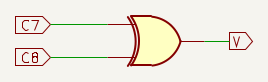
- C7 and C8 are inverted with respect to each other, i.e. C7 <> C8 (in this case too a relative comparison is performed);
- (A7 = B7’ = 1 AND Q7 = 0) OR (A7 = B7’ = 0 AND Q7 = 1) is similar to the first point, but, instead of placing the bits in a relative comparison, we are specifying their absolute value.
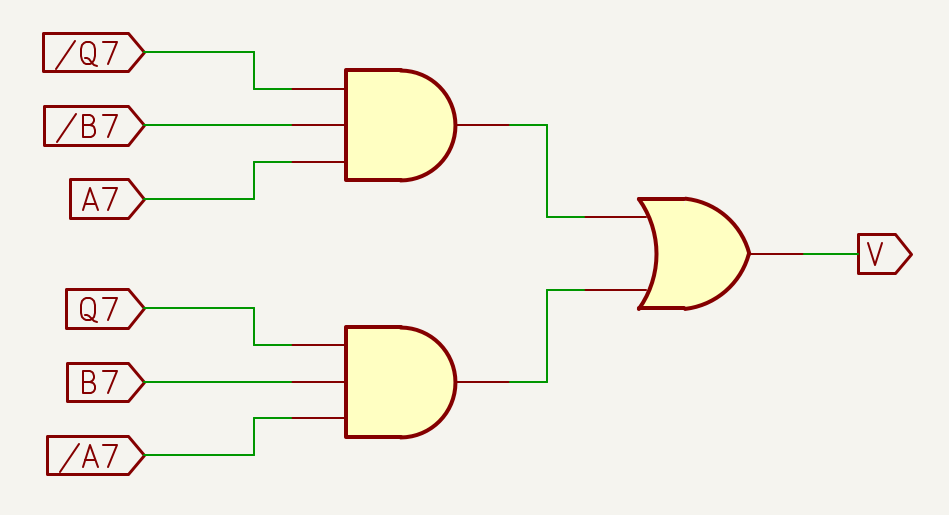
The truth table (A7 == B7’) AND (A7 <> Q7) of the first case would translate into the logic shown in the figure; unfortunately, the computer based on the 74LS181 does not offer visibility of the value of B7’, which is computed internally to the ALU and not exposed, therefore this method is not usable:
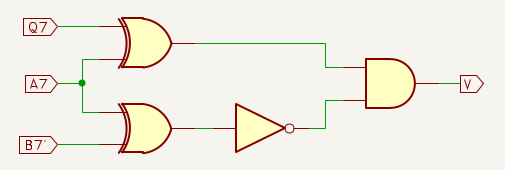
For the sake of completeness 😊 I include the schematic of two registers A and B and a generic Half Adder that I had drawn to better understand additions; note the circuitry designed to identify Overflow situations.

In the second case C7 <> C8 as well, information is missing, because C7 is computed internally to the ALU and not exposed:
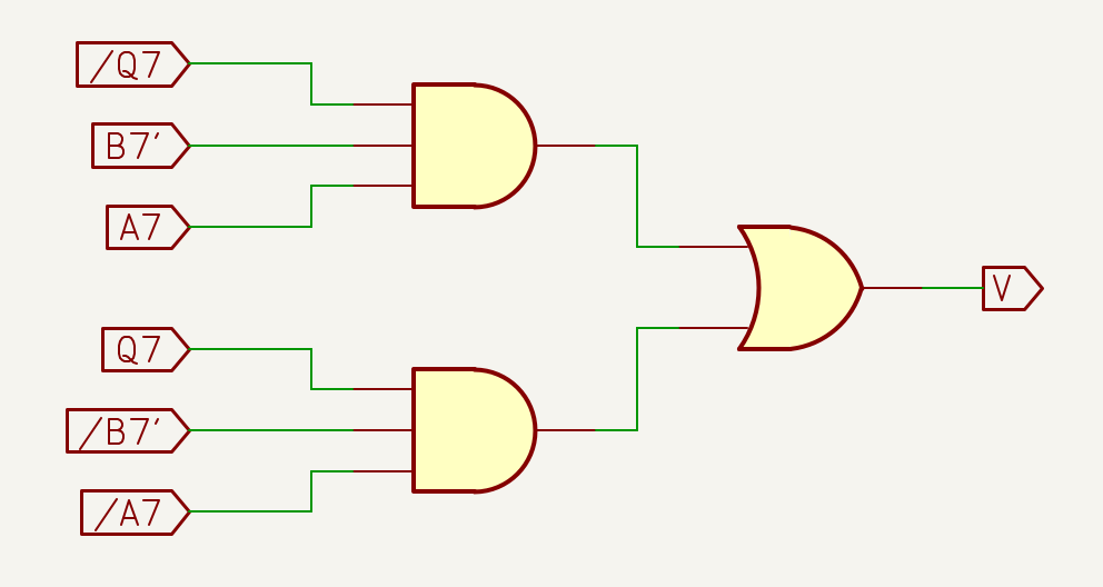
The third method (A7 = B7’ = 1 AND Q7 = 0) OR (A7 = B7’ = 0 AND Q7 = 1) also does not seem usable, because B7’ is confined to the internal circuitry of the ALU:
The three methods examined seem to lead to a dead end; however, it is possible to artificially reconstruct the B7’ signal based on the other signals available in the computer
- In an addition, the B7’ value at the input of the last Adder of the ‘181 is equal to the value of B7 given as input to the chip (in an addition A7 + B7, B7’ does not undergo modifications from the ALU’s internal circuitry and we can therefore use B7 as input to the circuit that determines the possible Overflow state).
Some considerations allow reusing the same method also for verifying Overflow in subtractions. In fact, in the sections Sources and Unsigned and Signed Numbers on this page we have learned how a subtraction can be performed by carrying out an addition between the minuend and the two’s complement of the subtrahend, therefore:
- The B7’ value at the input of the last Adder of the ‘181 is inverted with respect to the value of B7 given as input to the chip (in a subtraction A7 - B7, B7’ is inverted by the ALU’s internal circuitry and we can therefore use the inverse of B7 as input to the circuit that determines the possible Overflow state):
In conclusion, the third method is usable for verifying Overflow both for additions and for subtractions.
At this point, we can implement a circuit capable of detecting overflow. It is necessary to integrate instruction management: the overflow detection circuit for additions must include a check that verifies whether the operation being executed is an addition; the same applies to subtraction.
Simplification with 74LS151
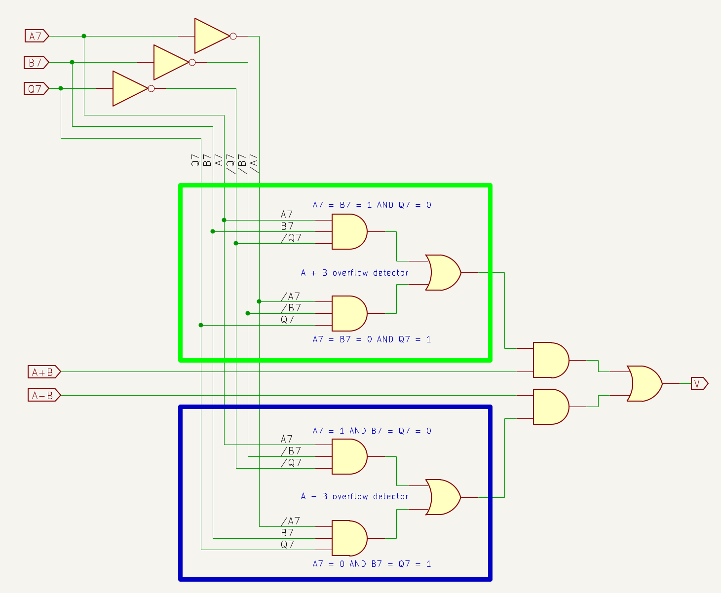
Now things get interesting: Dieter continues by indicating that a single 74LS151 chip, appropriately connected to the inputs A, B, Q, A + B and A - B, is capable of identifying all Overflow situations.
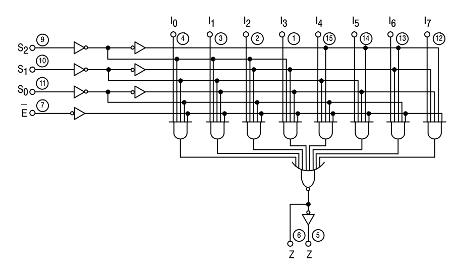
74LS151 logic schematic.
Let us highlight the two points to take into consideration to see if we can make them match with the ‘151:
- the Overflow equation is based on 3 inputs (A, B, Q);
- the possible Overflow is also a consequence of the operation performed; the Instruction Register can tell us whether an addition or subtraction is being executed.
A concrete example with equal inputs, but different situations:
- if A = 1, B = 1 and Q = 0 and we are performing an addition, we have an Overflow;
- if A = 1, B = 1 and Q = 0 and we are performing a subtraction, then there is no Overflow.
In fact, the ‘151 allows selecting a data source (among the 8 available I0-I7) based on a unique encoding presented to its selection inputs S2-S1-S0.
Trying to write a logical flow:
- the presence of a specific logic state at the selection inputs S2-S1-S0 connected to Q7, B7 and A7
- activates a specific input Ix among those connected to the Instruction Register, which
- thanks to the appropriate choice of the opcode of addition and subtraction instructions
- can result in a logic state 1 on the Z output of the ‘151
- highlighting an Overflow condition.
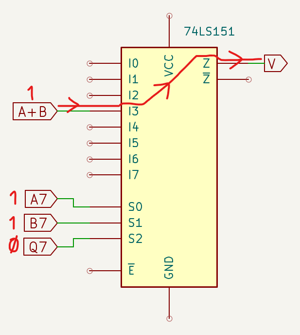
Let us assume for example that we are performing an addition with:
- ALU inputs A7 = B7 = 1 and output Q7 = 0, i.e. two negative Signed inputs and one positive Signed output, which determine an Overflow situation;
- I3 of the ‘151 connected to an Instruction Register line active in the case of an A + B addition instruction.
The combination 011 at the S2-S1-S0 inputs of the ‘151 will activate input I3, which will bring to output Z the signal at logic state 1 coming from the IR, highlighting an Overflow situation.
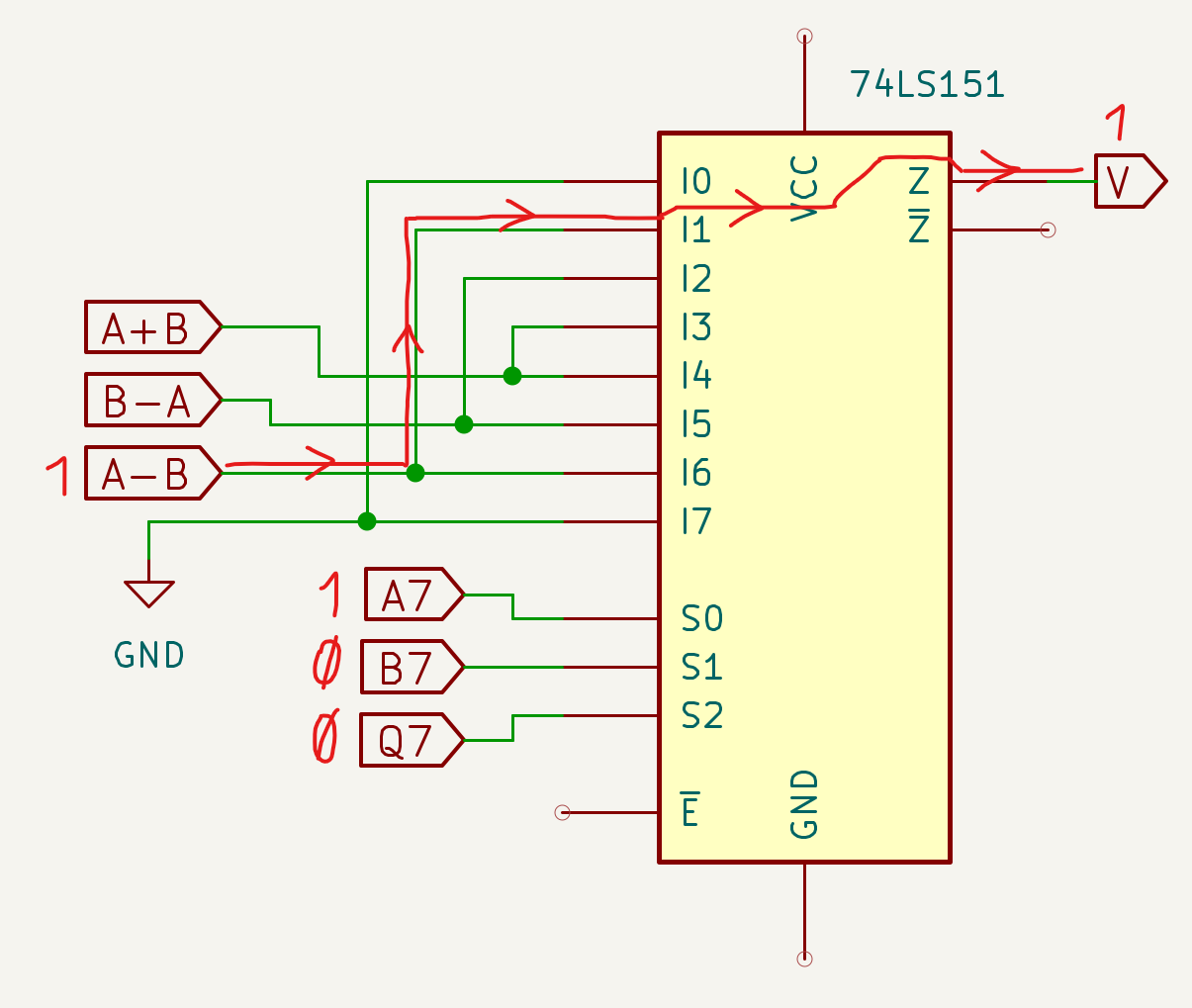
Having to address 8 combinations of Q, B and A (000, 001 etc. up to 111), a pin input configuration as highlighted in the following figure resolves the Overflow equations for both A + B additions and A - B and B - A subtractions, provided that pins I0-I7 of the ‘151 are correctly connected to the IR to detect the execution of A + B addition and A - B and B - A subtraction instructions:
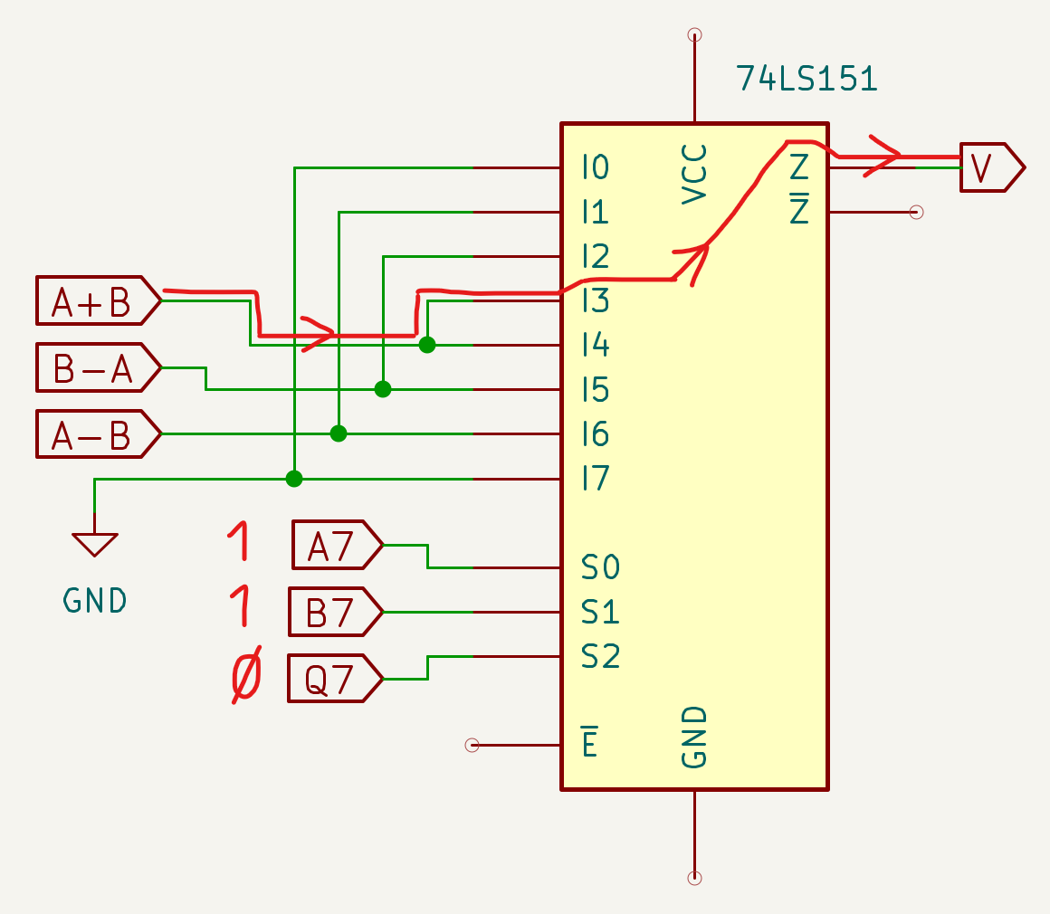
The following table summarizes the Overflow situations based on the states of Q, B and A and whether additions or subtractions are being performed:
| Q7-S2 | B7-S1 | A7-S0 | Sum/Sub | Input | Overflow |
|---|---|---|---|---|---|
| 0 | 0 | 0 | I0 | - | |
| 0 | 0 | 1 | A - B | I1 | 1 |
| 0 | 1 | 0 | B - A | I2 | 1 |
| 0 | 1 | 1 | A + B | I3 | 1 |
| 1 | 0 | 0 | A + B | I4 | 1 |
| 1 | 0 | 1 | B - A | I5 | 1 |
| 1 | 1 | 0 | A - B | I6 | 1 |
| 1 | 1 | 1 | I7 | - |
Note however that the B - A operation is not necessary to simulate the 6502 subtraction instructions.
In summary:
-
the combinations of the S2-S1-S0 inputs of the ‘151 (connected to the MSBs Q7, B7 and A7 of registers A and B and the ALU Q output) select which of the inputs I0-I7 needs to be activated to bring to the output a possible Overflow signal;
-
some of the inputs I0-I7 are appropriately connected in “Hardwired” mode to the Instruction Register to determine the operation currently being executed.
Addition and subtraction verification with 74LS151
Let us test some cases of addition and subtraction between A and B. In rows C and Q, the Carry, when present, and the result of the operation are indicated respectively.
- In the Hex column the hexadecimal representation of the numbers we want to add or subtract is shown, with the operation symbol to the left of the second number; we want to perform the operation 0x70 - 0x30.
- The Dec column shows the decimal value derived from the table Relationship between 8-bit Hex, Bin, Signed and Unsigned numbers; 0x70 corresponds to decimal 112, while 0x30 corresponds to 48: the operation is therefore 112 - 48 (which will have 64 as its result).
- The Bin column shows the binary representation of the numbers (in two’s complement if negative): 112 corresponds to 0111.0000, while 48 corresponds to 0011.0000.
- Note: if instead of a subtraction 112 - 48 we had wanted to perform for example an addition 112 + (-48) between a positive Signed and a negative Signed, the -48 would have been represented here in the column in its two’s complement form, i.e. 1101.0000.
- The 2C column is finally used to perform the addition operation by inverting the possible positive subtrahend: the subtrahend 48 is converted to 2C 1101.0000 (which in decimal is -48) and added to the minuend.
    Hex        Dec        Bin             2C
C                                        1111
A   0x70  ==>   112  ==>  0111.0000  ==>  0111.0000 +
B  -0x30  ==>   -48  ==>  0011.0000  ==>  1101.0000 =
               ----                      ----------
Q                64                      10100.0000 ==> 0100.0000 ==> 0x40 = 64, no Overflow
As reported on several occasions, the subtraction of a positive number (in our case 48) is performed by adding the minuend with the inverted value of the subtrahend, i.e. -48; the great advantage of two’s complement is precisely that of allowing the transformation of a subtraction into an addition, therefore the original operation 112 - 48 becomes 112 + (-48), i.e. 0111.0000 + 1101.0000 in the 2C column. In the result, the possible 9th bit must be discarded, since the calculation is performed on an 8-bit word; the 8th bit (MSB) of the result represents the sign, which in our example is 0 to indicate a positive Signed number.
In other words: when I need to perform the subtraction of a positive number, I calculate its two’s complement and add it to the minuend.
In the specific case of this example subtraction, there is no Overflow, since the value 64 resulting from the subtraction 0x70 - 0x30 is included in the range of 8-bit Signed numbers.
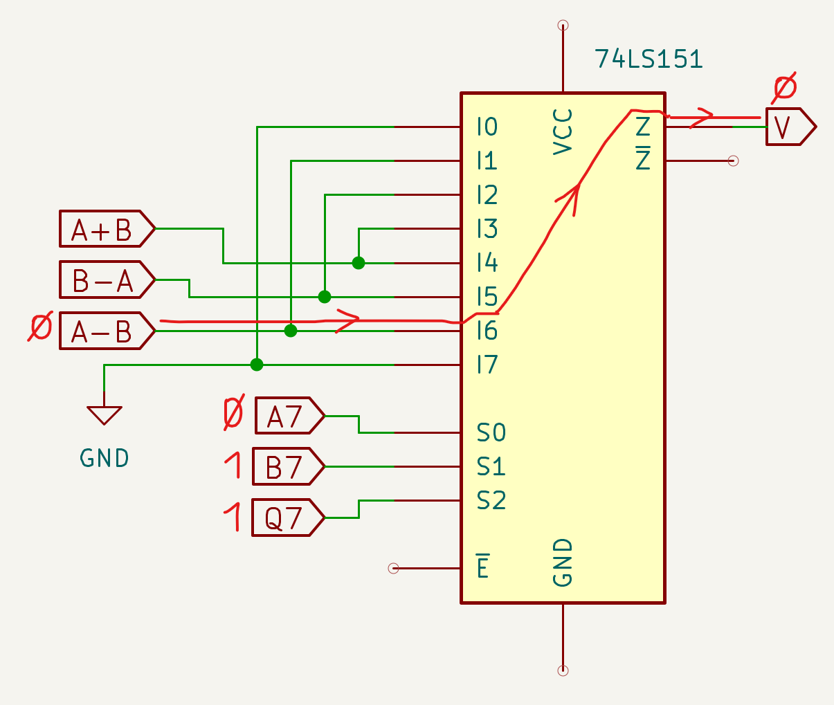
- Case 1: 0x20 + 0xC0; A + B addition of a positive Signed and a negative Signed.
    Hex        Dec        Bin             2C
C
A   0x20  ==>    32  ==>  0010.0000  ==>  0010.0000 +
B  +0xC0  ==>   -64  ==>  1100.0000  ==>  1100.0000 =
               ----                      ----------
Q               -32                       1110.0000 ==> 0xE0 = -32, no Overflow
The appropriately encoded microcode of the A + B instruction would bring inputs I3 and I4 of the ‘151 to 1, while all other inputs would be at 0; the operation would produce Q7=1, B7=1 and A7=0 on the selection inputs (S2-S1-S0 = 110), which would activate input I6 which is at 0 since it is not activated by the microcode, therefore the Q output of the ‘151 would be at 0, indicating that there is no Overflow –> situation correctly verified:
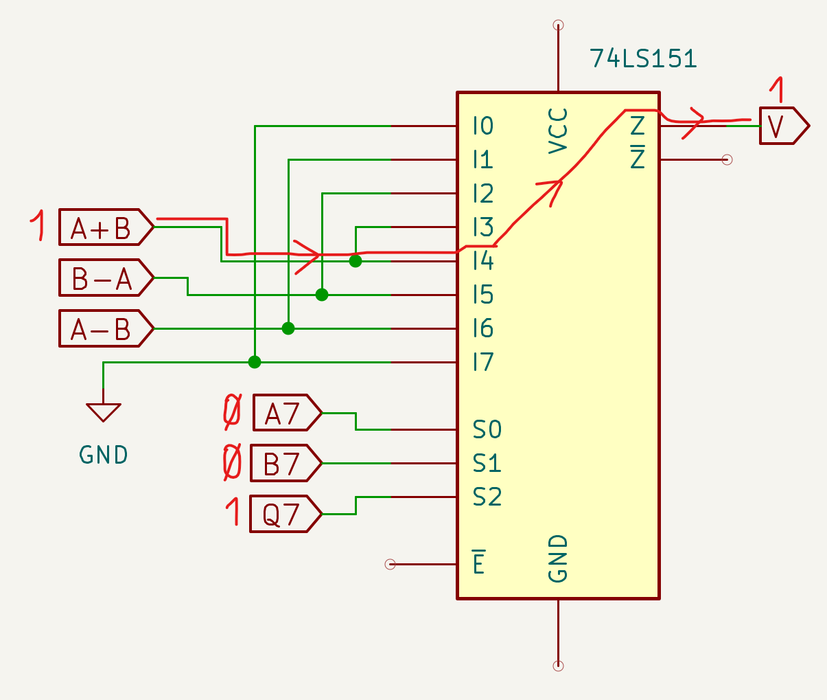
- Case 2: 0x20 + 0x70; A + B addition of two positive Signed numbers.
    Hex        Dec        Bin             2C
C                                         11
A   0x20  ==>    32  ==>  0010.0000  ==>  0010.0000 +
B  +0x70  ==>   112  ==>  0111.0000  ==>  0111.0000 =
               ----                      ----------
Q               144                       1001.0000 ==> 0x90 = -112, Overflow
The appropriately encoded microcode of the A + B instruction would bring inputs I3 and I4 of the ‘151 to 1, while all other inputs would be at 0; the operation would produce Q7=1, B7=0 and A7=0 on the selection inputs (S2-S1-S0 = 100), which would activate input I4 which is at 1 since it is activated by the microcode, therefore the Q output of the ‘151 would be at 1, indicating that there is Overflow –> situation correctly verified.
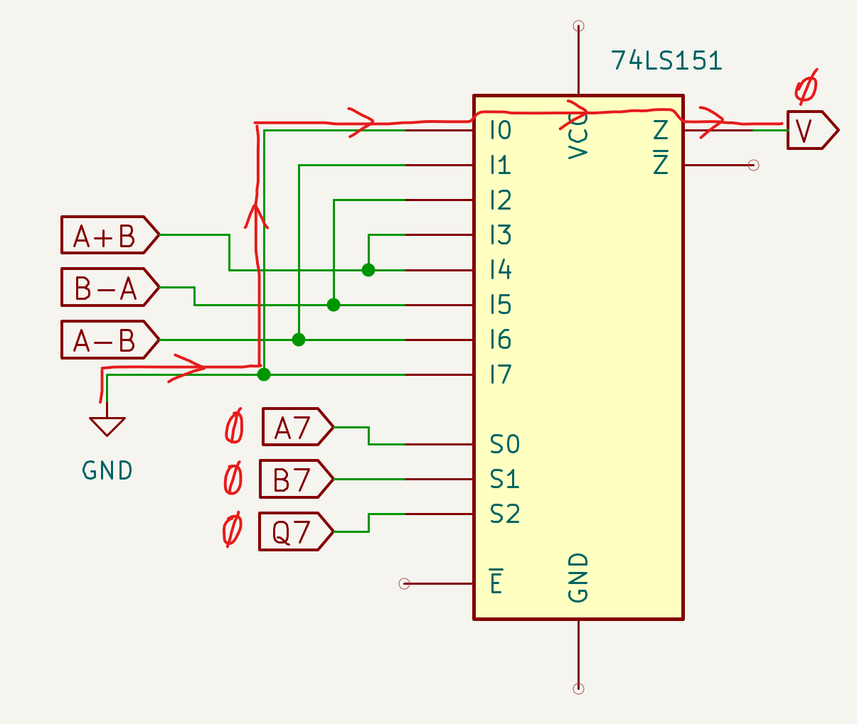
- Case 3: 0x50 - 0x30; A - B subtraction between two positive Signed numbers.
    Hex        Dec        Bin             2C
C                                        11 1
A   0x50  ==>    80  ==>  0101.0000  ==>  0101.0000 +
B  -0x30  ==>   -48  ==>  0011.0000  ==>  1101.0000 =
               ----                      ----------
Q                32                      10010.0000 ==> 0010.0000 ==> 0x20 = 32, no Overflow
The appropriately encoded microcode of the A - B instruction would bring inputs I1 and I6 of the ‘151 to 1, while all other inputs would be at 0; the operation would produce Q7=0, B7=0 and A7=0 on the selection inputs (S2-S1-S0 = 000), which would activate input I0 which is at 0, therefore the Q output of the ‘151 would be at 0, indicating that there is no Overflow –> situation correctly verified.
- Case 4: 0x90 - 0x30; A - B subtraction between a negative Signed and a positive Signed.
    Hex        Dec        Bin             2C
C                                        1  1
A   0x90  ==>  -112  ==>  1001.0000  ==>  1001.0000 +
B  -0x30  ==>   -48  ==>  0011.0000  ==>  1101.0000 =
               ----                      ----------
Q              -160                      10110.0000 ==> 0110.0000 ==> 0x60 = 96, Overflow
The appropriately encoded microcode of the A - B instruction would bring inputs I1 and I6 of the ‘151 to 1, while all other inputs would be at 0; the operation would produce Q7=0, B7=0 and A7=1 on the selection inputs (S2-S1-S0 = 001), which would activate input I1 which is at 1 since it is activated by the microcode, therefore the Q output of the ‘151 would be at 1, indicating that there is Overflow –> situation correctly verified.
Returning to the explanation of the example worked through at the head of the four cases just discussed, note that cases 3 and 4 are also subtractions in which the subtrahend is positive: in both cases the ALU will internally perform an addition of the minuend in its original state and the subtrahend inverted with two’s complement.
Returning then to the hardware interpretation, we have anticipated that the ALU modules of the NQSAP computer and the BEAM computer use only the A + B and A - B instructions, therefore we can simplify the ‘151 connections by eliminating B - A:
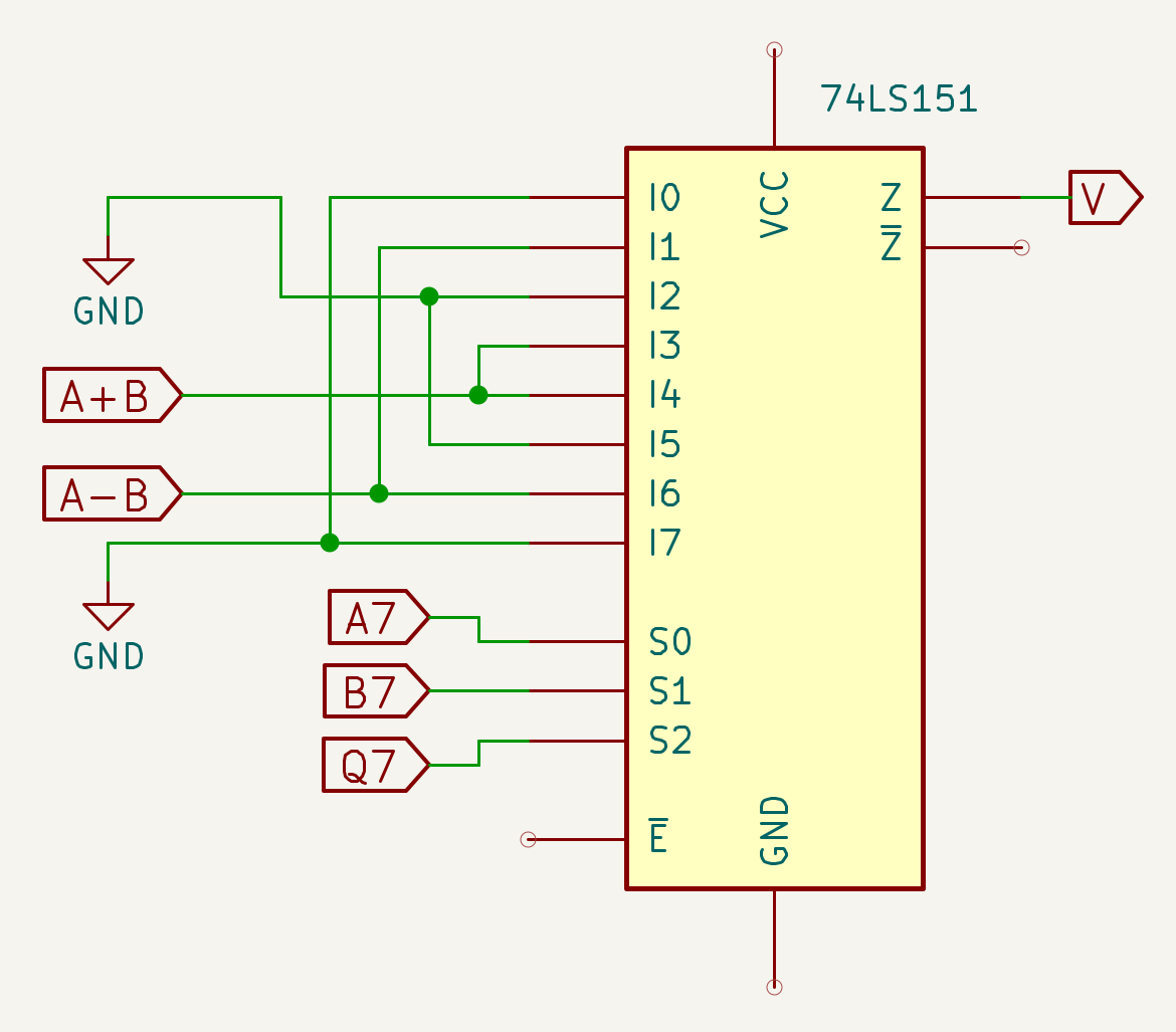
The (A + B) and (A - B) signals will need to have a hardwired connection with the Instruction Register to allow us to identify the addition and subtraction instructions respectively. When in the description of the four cases just seen it states “The appropriately encoded microcode…” it is in fact meant that these instructions will need to respect constraints in the choice of opcodes, so that we can know with certainty whether we are executing one or the other.
Returning to the schematic in the Overflow section from the Flag module page, we can now apply what we have seen on this page to understand its operation and visualize the final truth table:
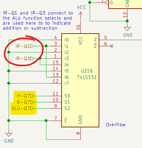
Use of the 74LS151 in the NQSAP for Overflow calculation with highlight of the MSBs of H, B and the ALU and the operation selection inputs IR-Q1 and IR-Q3.
In light of all the considerations made, this table can now take on a simpler meaning than what might have initially been thought:
| Q7-S2 | B7-S1 | A7-S0 | Sum/Sub | Input | Overflow |
|---|---|---|---|---|---|
| 0 | 0 | 0 | I0 | - | |
| 0 | 0 | 1 | A - B | I1 | 1 |
| 0 | 1 | 0 | I2 | - | |
| 0 | 1 | 1 | A + B | I3 | 1 |
| 1 | 0 | 0 | A + B | I4 | 1 |
| 1 | 0 | 1 | I5 | - | |
| 1 | 1 | 0 | A - B | I6 | 1 |
| 1 | 1 | 1 | I7 | - |
The Overflow flag is activated if:
- (A7 = B7 = 1 AND Q7 = 0) AND we are performing an addition (IR-Q3 active), or
- (A7 = B7 = 0 AND Q7 = 1) AND we are performing an addition (IR-Q3 active), or
- (A = 1 AND B = 0 AND Q = 0) AND we are performing a subtraction (IR-Q1 active), or
- (A = 0 AND B = 1 AND Q = 1) AND we are performing a subtraction (IR-Q1 active).
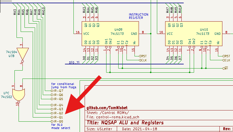
To identify the execution of an addition or subtraction operation, two lines of the Instruction Register are used:
| IR-Q3 | IR-Q1 | Operation |
|---|---|---|
| LOW | HIGH | Subtraction |
| HIGH | LOW | Addition |
In other words, the opcodes of the addition and subtraction instructions will need to have bits 1 and 3 set as shown in the table, while the other bits will not have such constraints:
| bit | Addition | Subtraction |
|---|---|---|
| 0 | X | X |
| 1 | LOW | HIGH |
| 2 | X | X |
| 3 | HIGH | LOW |
| 4 | X | X |
| 5 | X | X |
| 6 | X | X |
| 7 | X | X |
This corresponds exactly to what is indicated in the section A practical example of the ALU module page, in which it is highlighted for example that addition instructions will need to present “01001 on the 5 bits shared between the Instruction Register and the ALU”: bit number 3 is at 1, while bit number 1 is at 0, exactly as required by the previous table.
Finally, from what we have seen up to now we can deduce another rule: the addition of two Signed numbers of opposite sign and the subtraction of two Signed numbers of the same sign cannot cause Overflow.
Adders
We have discussed additions and subtractions, almost taking for granted that circuits exist that implement them. A mention can be found in a schematic in the section Overflow identification methods, but we are not satisfied and want to know more. How are additions performed? And subtractions?
An Adder is a basic logic unit that allows performing additions and, when appropriately configured, subtractions.
Additions with the Adders
What are the possible cases of additions between two bits A and B?
Hypotheses  1st    2nd    3rd    4th
C                               1
A           0+     0+     1+     1+
B           0=     1=     0=     1=
          ----   ----   ----   ----
Q           0      1      1     10
In the fourth hypothesis we note that the addition of two bits both equal to 1 generates a carry, i.e. a Carry “C”. Writing the truth table and considering the Carry generated by the addition of bits A and B, we obtain:
| A | B | Q | COUT |
|---|---|---|---|
| 0 | 0 | 0 | 0 |
| 0 | 1 | 1 | 0 |
| 1 | 0 | 1 | 0 |
| 1 | 1 | 0 | 1 |
The result Q of the addition of the two bits A and B can be obtained with an XOR logic gate, while the Carry COUT is clearly obtainable with an AND gate. Here is how the equivalent circuit could be built
Half Adder.
The circuit just created is called a Half Adder. The Carry, when active, highlights an overflow situation, i.e. a result of the operation that exceeds the representation capacity permitted by the available bits.
Let us now assume we want to perform a multi-bit addition, for example of two nibbles (4 bits) or two bytes:
C       1 11           1  1
A        1011+        10110011+
B        1001=        00101010=
        ------       ----------
Q       10100         11011101
Note that to perform the entire operation it is necessary to provide the Adder with 3 input values: A, B and the Carry possibly derived from the previous column.
Writing the truth table to add the three bits of each column, we will assign the name CIN to the carry derived from the previous column and, similarly, we will call COUT the carry resulting from the addition of each triplet CIN, A and B:
| CIN | A | B | Q | COUT |
|---|---|---|---|---|
| 0 | 0 | 0 | 0 | 0 |
| 0 | 0 | 1 | 1 | 0 |
| 0 | 1 | 0 | 1 | 0 |
| 0 | 1 | 1 | 0 | 1 |
| 1 | 0 | 0 | 1 | 0 |
| 1 | 0 | 1 | 0 | 1 |
| 1 | 1 | 0 | 0 | 1 |
| 1 | 1 | 1 | 1 | 1 |
Rather than resorting to the combination of AND and OR (Sum of Products, presented in Brock LaMeres’ video Combinational Logic Synthesis: SOP Forms & Minterms), let us try to simplify using Karnaugh maps (explained in the video Combinational Logic Minimization: K-map Formation, also by LaMeres).
The analysis of Q produces the following map (in which C corresponds to the CIN seen in the truth table):
Although it is not possible to simplify the truth table because it is not possible to create groups of 1s, the “checkerboard” pattern can be noted, which indicates that the equivalent logic circuit is an XOR gate with three inputs (see the video Combinational Logic Minimization: XORs, also by LaMeres).
The analysis of COUT produces this other map (in which, as before, C corresponds to the CIN seen in the truth table)
Using the distributive property of boolean algebra, it is possible to simplify the function
F = B*CIN + A*CIN + A*B to
F = CIN*(A+B) + A*B, i.e.
COUT = CIN*(A+B) + A*B
Having the 2-bit Adder seen previously at our disposal, the question now arises as to whether it might not be possible to reuse it at scale to simplify the construction of an Adder capable of performing additions between words of length for example 4 bits, 8 bits and so on.
Let us try to answer the question. It has been seen that each Half Adder provides an XOR gate and an AND gate, both with two inputs.
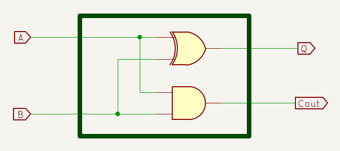
1) To implement the sum Q an XOR gate with three inputs is needed, but it can be demonstrated that two XOR gates with two inputs placed in cascade produce the same result. In fact, assuming we have two Half Adders, it is possible to obtain the result Q by exploiting the two available XOR gates:
Two Half Adders.
2) To implement COUT we must instead implement the function F = CIN*(A+B) + A*B
A*B is available on the output of the AND gate of the first Adder; CIN*(A+B) requires an OR between A and B and a subsequent AND with CIN. Unfortunately, neither of the two Adders provides an OR gate to perform (A+B); however, it can be demonstrated that the function:
COUT = CIN*(A+B) + A*B, not implementable with the available gates, is equivalent to the function
COUT = CIN*(A⊕B) + A*B, implementable with the available gates (note the substitution of the OR “+” with the XOR “⊕”).
| CIN | A | B | A*B | A⊕B | A+B | Q | CIN*(A+B) | CIN*(A+B) |
CIN*(A⊕B) | CIN*(A⊕B) |
|---|---|---|---|---|---|---|---|---|---|---|
| 0 | 0 | 0 | 0 | 0 | 0 | 0 | ||||
| 0 | 0 | 1 | 0 | 1 | 1 | 1 | ||||
| 0 | 1 | 0 | 0 | 1 | 1 | 1 | ||||
| 0 | 1 | 1 | 1 | 0 | 1 | 0 | ||||
| 1 | 0 | 0 | 0 | 0 | 0 | 1 | ||||
| 1 | 0 | 1 | 0 | 1 | 1 | 0 | ||||
| 1 | 1 | 0 | 0 | 1 | 1 | 0 | ||||
| 1 | 1 | 1 | 1 | 0 | 1 | 1 |
As can be seen from the truth table, the output of the third-to-last column CIN*(A+B) + A*B is equal to that of the last column CIN*(A⊕B) + A*B, therefore, we can use the Half Adder with XOR gate to complete our improved Adder.
At this point, we can implement the necessary function by adding a simple OR gate to perform the logical sum between CIN*(A⊕B) and A*B.
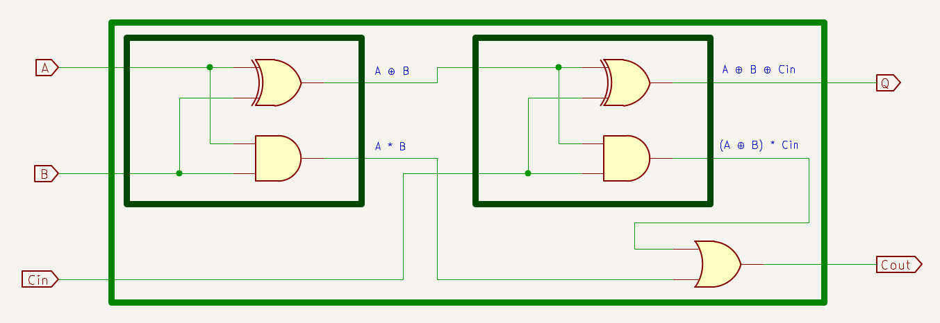
Full Adder.
The Full Adder just created is capable of performing the addition of two terms taking into account the input Carry and generating a possible output Carry.
Multiple Bit Adder
To perform multi-bit additions, Multiple Bit Adders are used. The role of the Carry in Adders is fundamental and there are at least two methods of managing the Carry. In the following sections the Ripple Carry Adder and Carry Look Ahead modes are described, also implemented in the 74LS181 used in the ALU.
Ripple Carry Adder
Having the Full Adders consisting of two Half Adders and an OR gate at our disposal, we can now create a Multiple Bit Adder to perform additions of nibbles, bytes and, more generally, words of any size. It will be noted that this paragraph allows a positive answer to the question that asked us about the possibility of implementing a complex circuit starting from a simple and repeatable basic logic.
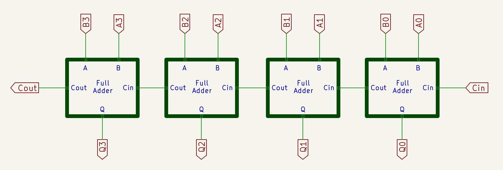
4-bit Multiple Bit Adder, or Ripple Carry Adder.
The arrangement of the Multiple Bit Adder in the figure follows the order of presentation of binary numbers, with the most significant bit on the left and the least significant on the right. The CIN must be kept at LO state, so the result of the operation will depend exclusively on the inputs present in A0-A3 and B0-B3.
The Multiple Bit Adder created has a unique name: Ripple Carry Adder (RCA), because the Carry “ripples”, it moves between the Full Adders. A consideration not to be overlooked is, in fact, that relating to timing: as with any logic circuit, we can sample the output signals only once the output with the greatest delay has stabilized.
The following image, taken from the video Ripple Carry Adders Timing, helps visualize how the COUT signal depends on as many as 9 levels (in the analysis of a circuit, the worst case must be considered).
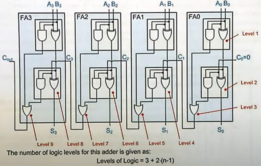
Timing of a Ripple Carry Adder.
Consequently, the maximum operating frequency of the circuit cannot exceed the inverse of the sum of the delays introduced by levels 1-9.
Carry Look Ahead Adder
A Carry Look Ahead (CLA) Adder addresses the problem of delay caused by the long chain of levels present in a Ripple Carry Adder.
If in a 4-bit Ripple Carry Adder the delay may be modest, the delay in a 16-bit or larger Adder can significantly reduce the maximum operating frequency. In fact, every Full Adder in an RCA depends on the result of the previous Adder; having to consider the worst case, the result of the last Full Adder depends on all the previous Full Adders.
To address the problem just described, it is necessary that each Full Adder can calculate its own Carry Out independently of the Carry Out made available by the previous stage. For this to happen, circuitry capable of calculating its own Carry In must be added to each Full Adder, without using the Carry Out of the previous Full Adder.
Clearly, this leads to a trade-off: the response speed of each Full Adder increases, at the cost of increased complexity due to the greater number of logic gates.
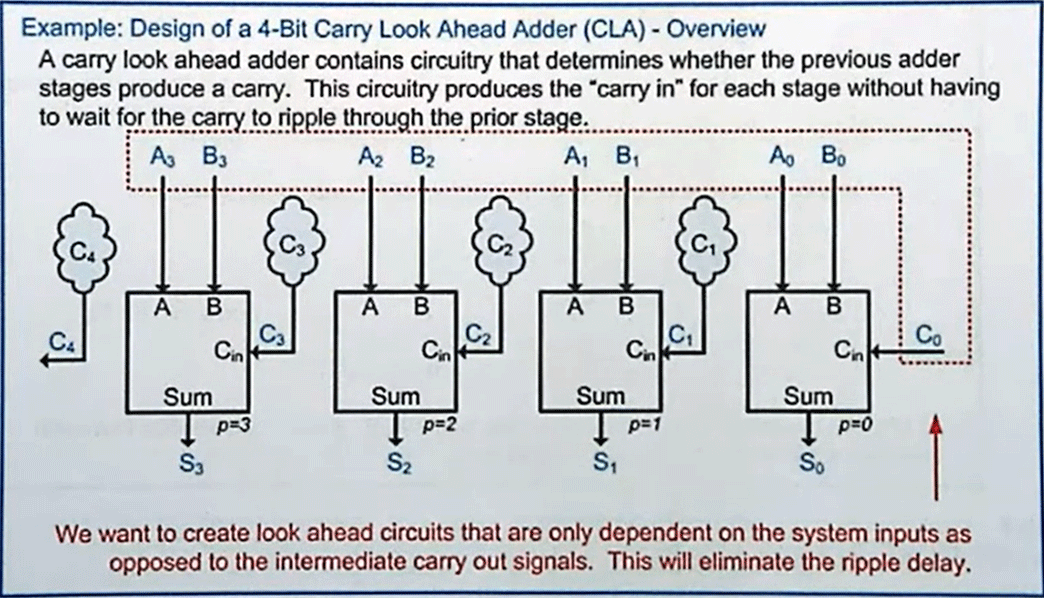
Carry Look Ahead Adder.
The image shows that the inputs of the various stages of a Carry Look Ahead Adder (CLA) depend only on terms A and B and on Carry C0; this is possible thanks to a series of algebraic substitutions that allow each individual Full Adder to compute its own sum and its own Carry Out starting from inputs A, B and from C0.
In other words, logic dependent only on terms A and B and on Carry C0 is created. How is this result achieved?
By identifying the situations in which a Carry is generated or propagated, each Adder(i) can be equipped with a circuit capable of knowing whether it will find an input Carry by computing it starting from the inputs of all the previous Adders and from C0, i.e. without depending on what is present at the output COUT of the previous Adder(i-1).
An answer must be found to the key question “in which situations does an Adder(i) find a Carry In equal to 1 at its input?”
Reducing this concept to logical expressions, two are the cases to analyze:
- In which situations does a Full Adder(i-1), whose Carry In is 0, certainly generates a Carry Out that is passed to the next Full Adder(i)?
- In which situations does a Full Adder(i-1) propagate a potential Carry In to the next Full Adder(i)?
The two situations just described are translated into expressions called Generate and Propagate.
-
In which cases does a Full Adder generate a Carry Out without a Carry being present at its Carry In input? Analyzing its truth table, we find that if CIN is 0, COUT is 1 only if both A and B are 1: therefore, to implement this circuit we can use an AND gate. This case is described with the expression g = A*B and can be read as “the Generate logic of each Full Adder corresponds to A AND B”.
-
When, instead, does a Full Adder propagate a Carry present at its Carry In input? If the CIN of that Adder is 1, COUT is 1 when A or B is 1: therefore, this circuit can be implemented using an OR gate. This case is described with the expression p = A+B and can be read as “the Propagate logic of each Full Adder corresponds to A OR B”.
Connecting the dots, for each position a Generate signal is created if both bits A and B are 1 and a Propagate signal if at least one of the two bits is 1:
| CIN | A | B | Q | COUT | Generate / Propagate |
|---|---|---|---|---|---|
| 0 | 0 | 0 | 0 | 0 | |
| 0 | 0 | 1 | 1 | 0 | |
| 0 | 1 | 0 | 1 | 0 | |
| 0 | 1 | 1 | 0 | 1 | Generate (A AND B) |
| 1 | 0 | 0 | 1 | 0 | |
| 1 | 0 | 1 | 0 | 1 | Propagate (A OR B) |
| 1 | 1 | 0 | 0 | 1 | Propagate (A OR B) |
| 1 | 1 | 1 | 1 | 1 | Propagate (A OR B) |
Truth table of a Full Adder.
In other words, the Look Ahead circuitry evaluates whether the previous stage introduces a Carry Out by analyzing the two previous conditions. Given inputs A, B and CIN:
- the Generate expression is used by an Adder “i” to identify when, in the absence of a Carry at the inputs of the previous stage “i-1”, it will produce (“generate”) a Carry COUT (condition verified only if A*B = 1), which Carry Out the Adder(i) will find at its Carry In;
- the Propagate expression is used by an Adder “i” to identify when, in the presence of a Carry at the inputs of the previous stage “i-1”, it will produce (“propagate”) a Carry COUT (condition verified only if CIN = 1 and A+B = 1), which Carry Out the Adder(i) will find at its Carry In.
At this point, we can identify the possible presence of the Carry Out of each stage with a generic expression:
COUT = g + p*CIN, i.e., by substituting g and p:
COUT = A*B + (A+B)*CIN, which we are already familiar with, as it is nothing other than COUT of any Full Adder.
We now use i to identify the position of each bit within the Multiple Bit Adder — for example, 0–3 for a 4‑bit adder—and write the general expressions for p and g:
gi = Ai*Bi (e.g., g2 = A2*B2)
pi = Ai+Bi (e.g., p3 = A3+B3)
Let us now compute the Carry‑In “C” of a generic adder i+1, which corresponds to the Carry Out of the preceding Adder i, by analyzing the inputs of the latter:
Ci+1 = gi + pi*Ci, i.e.
Ci+1 = Ai*Bi + (Ai+Bi)*Ci
We can now write the expressions for the Carry Ins of all stages. The expression for the Carry In of the second adder is:
C1 = g0 + p0*C0, i.e.,
C1 = A0*B0 + (A0+B0)*C0
Note that this expression depends only on the inputs A, B, and C0, which is exactly what we want to achieve: do not depend on the Carry Out of the preceding Adder.
We now proceed to write the expression for the Carry In the third Adder:
C2 = g1 + p1*C1
We need to eliminate C1, because we are trying to make each adder independent of the carry‑out of the preceding adder; therefore, by substituting C1:
C2 = g1 + p1*(g0 + p0*C0), which means that C2 does not depend on the result of the previous Adder, but only on the A and B inputs of the previous Adders and on C0. Applying the distributive property, we obtain:
C2 = g1 + p1*g0 + p1*p0*C0, i.e.:
C2 = A1*B1 + (A1+B1)*A0*B0 + (A1+B1)*(A0+B0)*C0
This expression too depends, therefore, only on inputs A, B and C0.
Let us proceed by writing the expression for the Carry In of the fourth Adder
C3 = g2 + p2*C2, i.e., by substituting C2:
C3 = g2 + p2*(g1 + p1*g0 + p1*p0*C0), which means that C3 does not depend on the result of the previous Adder, but only on the A and B inputs of the previous Adders and on C0. Applying the distributive property, we obtain:
C3 = g2 + p2*g1 + p2*p1*g0 + p2*p1*p0*C0, i.e.:
C3 = A2*B2 + (A2+B2)*A1*B1 + (A2+B2)*(A1+B1)*A0*B0 + (A2+B2)*(A1+B1)*(A0+B0)*C0
As in the previous cases, this expression too depends only on inputs A, B and C0. Let us finally write the expression for C4, which is the Carry Out of the fourth Adder:
C4 = g3 + p3*C3, i.e., by substituting C3:
C4 = g3 + p3*(g2 + p2*g1 + p2*p1*g0 + p2*p1*p0*C0), which means that C4 does not depend on the result of the previous Adder, but only on the A and B inputs of the previous Adders and on C0. Applying the distributive property, we obtain:
C4 = g3 + p3*g2 + p3*p2*g1 + p3*p2*p1*g0 + p3*p2*p1*p0*C0, i.e.:
C4 = A3*B3 + (A3+B3)*A2*B2 + (A3+B3)*(A2+B2)*A1*B1 + (A3+B3)*(A2+B2)*(A1+B1)*A0*B0 + (A3+B3)*(A2+B2)*(A1+B1)*(A0+B0)*C0
Observing the expressions of each Adder, it can be deduced that all depend only on inputs A, B and C0, which is exactly the goal to be pursued: each stage calculates its own Carry without having to wait for the Carry calculation performed by the previous stage.
Let us now implement a Carry Look Ahead Adder, but first, considering what we have seen above, let us modify the Full Adders by creating Modified Full Adders.
The sum Q, as always, corresponds to A0⊕B0⊕C0. We add to the Full Adder an OR gate and an AND gate with the sole purpose of obtaining the terms p (i.e. A0+B0 for the first Adder) and g (i.e. A0*B0 for the first Adder)
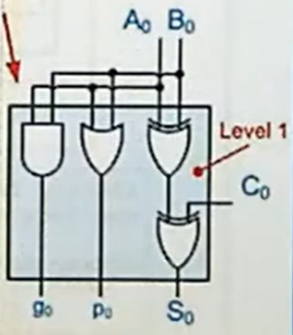
Logic of the sum of the Modified Full Adder.
Let us now add the logic of Carry C1 = g0 + p0*C0:
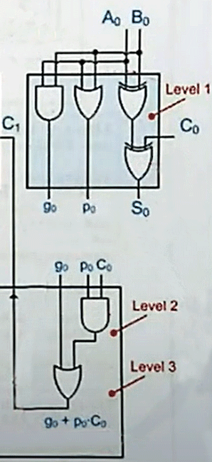
Logic of the Carry of the Modified Full Adder.
Note that the Carry Out C1 of the first Adder is at level 3, which means that the longest path is represented by an OR gate that has A0 and B0 as inputs, whose output p0 enters an AND gate, whose output enters a final OR gate from which C1 is obtained. In fact, at this point, we are in the same situation as the RCA, whose C1 was generated at the 3rd level.
Adding the next Modified Full Adder, it can be verified that the sum is computed at the 4th level, while the Carry is, as in the previous Adder, still computed at the 3rd level (OR gate at the bottom left).
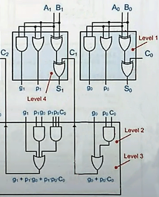
Two-stage Modified Full Adder.
Continuing with the third and fourth Modified Full Adder, the sum remains at the 4th level, while the Carry continues to be generated at the 3rd level.
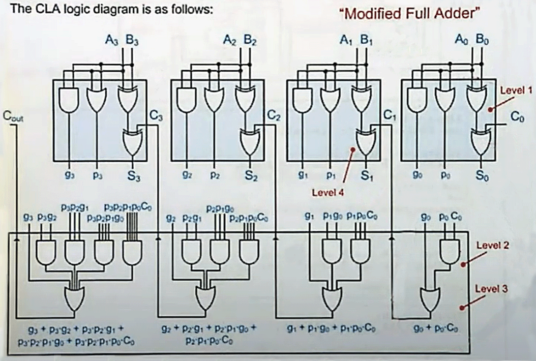
Four-stage Modified Full Adder.
As can be seen from the screenshots, used with the kind permission of professor Lameres, each subsequent Adder adds a lot of logic, but the Multiple Bit Adder created allows additions to be performed with a fixed number of levels regardless of the number of input bits, unlike the Ripple Carry Adder (for which, moreover, the addition of a word of just 4 bits required as many as 9 levels).
In conclusion, the work done to create the Carry in a CLA Adder is very high, but maximum performance is obtained in return.
One aspect to take into consideration could be the fan-in factor, which limits the number of inputs that a logic gate can have. The final OR gate, which generates the Carry Out, will have an ever-increasing number of inputs as the number of Adder bits increases, as will the AND gates connected to this OR. At a certain point it will be necessary to split the OR and AND gates into two levels, thus causing an increase of 2 levels in the total level count of the Adder. Therefore, the number of levels also increases as the number of bits of the CLA Adder increases, but at a significantly lower rate than that of the Ripple Carry Adder, in which each individual bit adds as many as two levels to traverse.
Implementation in the 74LS181
The 74LS181 internally implements a Carry Look Ahead mechanism slightly different from the one described in the previous section, but the basic concepts are similar (Propagate and Generate used to calculate the Carry of each position).
The Carry Look Ahead (CLA) mechanism in the ‘181 circuit can be somewhat counterintuitive, since it is closely tied to the S3/S0 selection signals that govern its 32 logic and arithmetic functions. A more straightforward representation to analyze can be found in the 4-Bit Binary Full Adder With Fast Carry 74LS283, designed exclusively for performing additions. Here, the CLA logic is considerably simplified: for each pair of input bits (A3/A0 and B3/B0), a NAND gate implements the Generate function, while a NOR gate implements the Propagate function.
When the word is longer than the 4 bits managed by a single chip, the RCA and CLA modes can be used for interconnecting multiple ALUs:
-
The RCA mode is the simplest to implement and consists of cascading multiple ALUs, connecting the Carry Out of each to the Carry In of the next, as shown in the dedicated section Carry, additions and subtractions of the ALU page.
-
The CLA mode requires the use of an external Look-Ahead Carry Generator 74S182, which identifies the presence of the Carry between multiple interconnected 74LS181s according to the schematic visible on page 5.
Subtractions with the Adders
Throughout this page, it has been learned that binary subtractions are performed by adding the minuend and the two’s complement of the subtrahend: instead of performing “A - B”, B is inverted and added to A, obtaining an “A + (-B)” operation.
So far so easy: we can use a Multiple Bit Adder, for example a Ripple Carry Adder or a Carry Look Ahead Adder, and input A and -B, i.e. the two’s complement of B. Let us recall that “to convert a positive number to negative it is sufficient to invert all the bits and add 1”.
How can we invert the bits of a binary number and add 1? The inversion can easily be performed by XOR logic.
| Ctl | B | Q |
|---|---|---|
| 0 | 0 | 0 |
| 0 | 1 | 1 |
| 1 | 0 | 1 |
| 1 | 1 | 0 |
Assuming we use a Ctl signal as a control signal, it can be noted that Q equals B if Ctl is 0, while Q equals the inverse of B if Ctl is 1: therefore, by setting Ctl, all the bits of the minuend B can be inverted.
The last step remains, i.e. adding 1. The first Adder of a Multiple Bit Adder is equipped with a Carry In signal that, as noted in the Ripple Carry Adder section, is normally at 0; by setting the Carry In to 1, we obtain the desired result.
Therefore, to negate a binary number by transforming it into its two’s complement, we can use XOR gates to invert all the input bits and the Carry In signal of the first Adder to add 1: Ben Eater illustrates this very clearly in the video ALU Design for the SAP-1 computer.
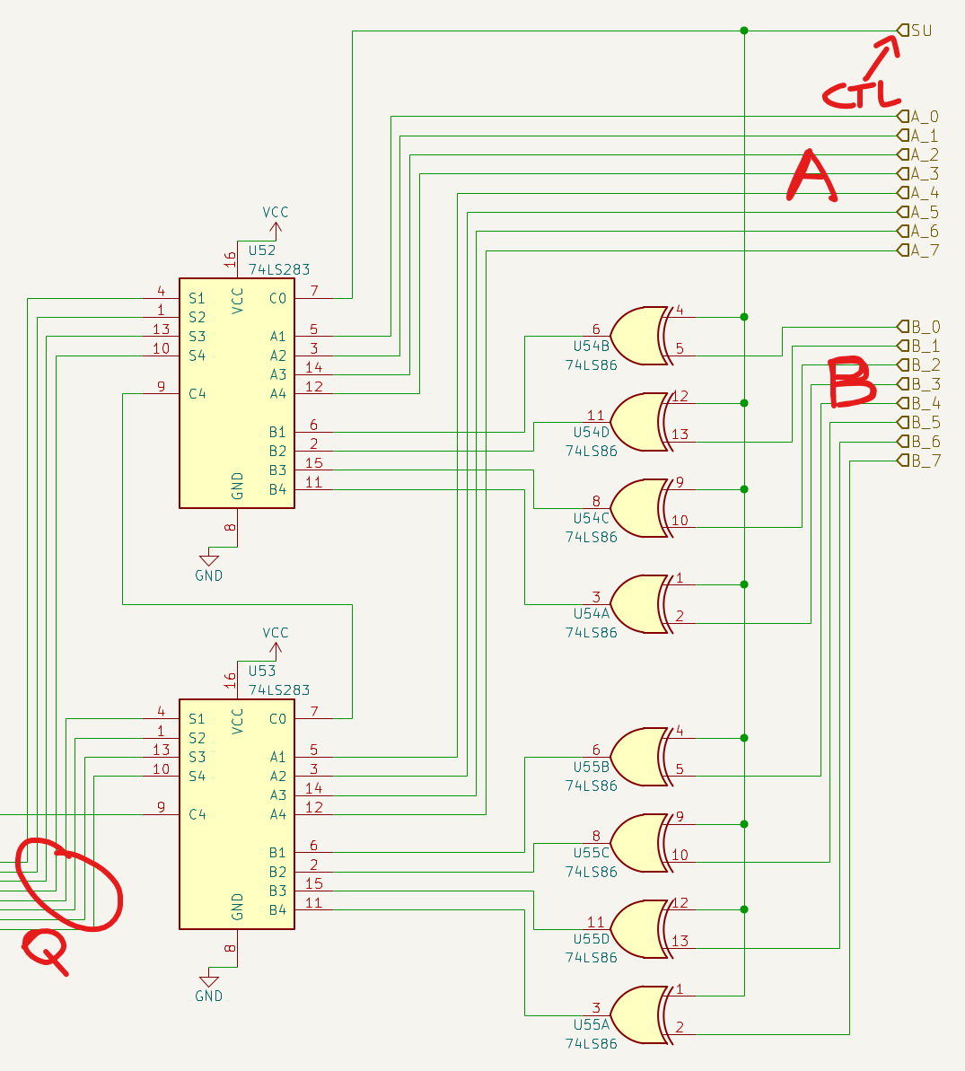
Detail of the Multiple Bit Adder inputs of Ben Eater’s SAP-1 Computer.
In the schematic we have two 4-bit 74LS283 RCAs in cascade and a Subtract signal (SU, renamed by us to Ctl) that allows selecting whether the B inputs should be normal or inverted and, simultaneously with the possible inversion, adding a Carry In to the first Adder, transforming B into its two’s complement to add it to A and finally perform the subtraction A + (-B).
Useful links
- Ripple Carry Adders (RCA), Ripple Carry Adders Timing and Carry Look Ahead (CLA) Adders by Brock LaMeres. These videos illustrate the logic of Half Adders and Full Adders, Ripple Carry Adders and Carry Look Ahead Adders. One cannot fail to mention the presentation style of professor LaMeres, whose great energy keeps the viewer glued to the video.
- The cryptic, but very interesting and extremely detailed analyses by Dieter Müller on Adders, Multiplexers and much, much more.
- The complete playlist Intro to Logic Circuits by Lameres, already suggested on the home page of the BEAM documentation.