EEPROM Programmer
The EEPROM Programmer - Schematic - Code Explanation - The EEPROMs and Their Content - Pre-Programming CRC Calculation - EEPROM Unlock and Lock - EEPROM erase - EEPROM Programming - Post-Programming CRC Verification - Notes - Useful links

The EEPROM programmer is used to program the Control Logic EEPROMs with the microcode needed to execute the instructions defined for the BEAM computer.
The EEPROM Programmer
My first experience with EEPROM programming dates back to the construction of Ben Eater’s SAP-1 computer and the realization of the programmer based on his schematics and sketches. This very simple project allowed the microcode EEPROMs to be programmed, although the writing process was particularly slow. Nevertheless, programming an EEPROM (first manually, then with the programmer) was an exhilarating moment — I never would have thought I could understand the (all things considered, fairly simple) mechanisms that made it possible.

Schematic of the SAP-1 computer EEPROM programmer.
While studying Tom Nisbet’s NQSAP computer and revisiting his project to create the BEAM computer, I had realized that the number of EEPROMs to be programmed (four instead of two) and their size would have further increased the programming time for each microcode revision. Ben’s programmer was functional, but did not take advantage of the page write feature of modern EEPROMs, which allows a 32KB EEPROM to be programmed in just a few seconds. Nevertheless, I continued to use it, with write times of several tens of seconds for each EEPROM.
As the construction of the BEAM modules progressed, the reprogramming operations needed to implement the Instruction Set and fix microcode bugs became increasingly frequent; the time spent waiting for the programming cycles to complete was starting to become frustrating.
One of Tom’s projects, the TommyPROM programmer, supported a variety of EPROMs, EEPROMs and Flash memories. This programmer included very feature-rich and very fast software thanks to its support for Page Write mode. A stripped-down version of the TommyPROM software — with the sole purpose of generating the microcode and programming the 28C256 EEPROMs — was published by Tom in his NQSAP repository.
I did not want to start a new EEPROM programmer project while I was still working on the BEAM. However, at a certain point I had realized that I would spend less time building a programmer based on the TommyPROM than the time I would waste continuing to use Ben’s basic programmer.

Schematic of Tom Nisbet’s TommyPROM EEPROM programmer.
My initial programmer was identical to the one developed by Ben for the SAP-1 and used the 74HC595 instead of the 74HCT164 used by Tom. In one section of the documentation, Tom pointed out that his code did not work on Ben’s design and that it required significant modifications. If one wanted the benefits of the TommyPROM on Ben’s hardware, Tom indicated that the easiest path was not to modify the software, but rather to adapt the hardware to make it identical to that of the TommyPROM.
In my stubbornness, I had opted for a compromise: only partially modifying the hardware developed in Ben’s initial project, while at the same time taking the opportunity to study and modify Tom’s software to make it compatible with my hardware, to which I wanted to apply the fewest possible changes. At that point I did not yet know that the revised programmer would see the light in a substantially limited amount of time, but that the correct implementation of Page Write mode and above all the errors found in the CRC calculation would require a rather demanding effort.
The minimum necessary modifications compared to the original SAP-1 programmer were the following:
- The Write Enable pin of the EEPROM (/WE) no longer controlled by Arduino’s D13 signal, but by A2.
- The Chip Enable pin of the EEPROM (/CE) no longer connected to ground (chip always active), but controlled by Arduino’s A0 pin.
- The Output Enable pin of the EEPROM (/OE) no longer connected to the Shift Register, but controlled by Arduino’s A1 pin.
In his documentation Tom explains that in Ben Eater’s programmer D13 controls the Write Enable signal. Since D13 is internally connected to the built-in LED on the Arduino, which blinks during boot, unwanted writes to the EEPROM could occur every time the programmer is powered on. This was not an issue with Ben’s sketch, since the EEPROM was completely reprogrammed on every run, overwriting any spurious writes. However, since the TommyPROM could also be used for read-only operations on an EEPROM, the initial unwanted writes could have caused problems — hence the need to control /WE with a signal other than D13.
Another aspect to consider was related to the Output Enable pin of the EEPROMs: the ‘164 Shift Registers do not have an intermediate buffer acting as a latch during loading. As a result, their outputs are immediately modified on every Rising Edge of the clock, exposing /OE to possible unwanted activations. Conversely, the 74HC595 allows serial loading of data into an internal latch and the simultaneous output of all new output states on the Rising Edge of a dedicated signal (RCLK), eliminating the risk of unwanted activations of /OE. However, during the implementation of the modifications to the programmer I had not fully understood this aspect and had decided to follow Tom’s indication, that is, to dedicate a specific Arduino output to the EEPROM’s /OE. In other words, the modification at point 3 could have been avoided, but at that point I had not realized it.
Another difference lay in the write mode of the Shift Registers: Ben’s programmer had the two SRs connected in cascade, whereas Tom’s used two distinct clock signals to select which SR to address. The very clever idea behind Tom’s modification allowed the outputs of the second SR alone to be modified without performing a full address shift, saving precious Arduino clock cycles. I had chosen not to incorporate this modification into the BEAM programmer and to continue with the full shift sequence, hoping to meet the very tight timing parameters required by the Page Write programming mode of the EEPROMs.
Schematic

Schematic of the BEAM computer EEPROM programmer.
Code Explanation
The BEAM EEPROM programmer, based on Tom’s NQSAP one, is not interactive, unlike the far more complete TommyPROM. Once started, it sequentially performs the following steps, at the end of which it is ready for a reset and the programming of a new EEPROM:
- Calculation of the checksum of the data to be written to the EEPROM
- EEPROM unlock
- EEPROM erase
- EEPROM programming
- EEPROM lock
- Calculation of the checksum by re-reading the written data and comparison with the value calculated in step 1
- Elapsed time printout
The EEPROMs and Their Content
To control the 42 control signals of the ALU, RAM, SP, registers, etc. (21 directly output from the EEPROMs + 21 demultiplexed by the 74LS138) four EEPROMs are required, each exporting an 8-bit word for a total of 32 bits (the physically required signals are actually 29, i.e. the 21 direct ones and 8 to control the ‘138, leaving 3 pins unused):
- one EEPROM provides 8 bits of output, so 4 are needed to simultaneously drive 29 signals;
- since each of the 256 BEAM instructions can consist of a maximum of 16 steps, EEPROMs of size 256 * 16 = 4096 bytes are required;
- to address 4096 bytes, 12 address pins are needed ((2^8 = 256 instructions) * (2^4 = 16 steps) = 2^12 = 4096), i.e. from A0 to A11;
- four 4KB EEPROMs, each programmed with its own microcode, can perform the required task.
Below we can see a detail of the microcode of some example instructions, in particular HLT (halts code execution), JMP (jumps to a new address defined in the memory location indicated by the operand) and CPX (compares the X register with the operand). The longest instruction among those shown is CPX, with a duration of 7 steps (from 0 to 6); other BEAM instructions reach a length of as many as 10 steps.
// Step:
// <0>     <1>         <2>     <3>    <4>        <5>            <6>
{  RPC|WM, RR|WIR|PCI, HLT,    NI,    0,         0,             0,           }, // 00 HLT
{  RPC|WM, RR|WIR|PCI, RPC|WM, RR|WM, RR|WPC|NI, 0,             0,           }, // 01 JMP
{  RPC|WM, RR|WIR|PCI, RPC|WM, RR|WB, RX|WH,     CS|C0|FNZC|RL, RA|WH|PCI|NI }, // 06 CPX
Microcode detail of some example instructions.
Each step enables one or more signals: for example, the seventh step of the CPX instruction simultaneously activates RA, WH (which in turn is composed of HL and HR), PCI and NI.
As can be seen in the Arduino sketch, each control signal corresponds to one or more specific pins in the three EEPROMs numbered 1, 2 and 3:

Definition of the control signals managed by each EEPROM.
Why one or more specific pins? Because, for example, the mnemonic WH is actually a macro that activates both HL and HR.
#define WH HR|HL // Write H
EEPROM 0 instead controls the four ‘138 demultiplexers, so the combinations of its 8 output bits are able to drive as many as 32 signals (but only 21 of them are actually used).
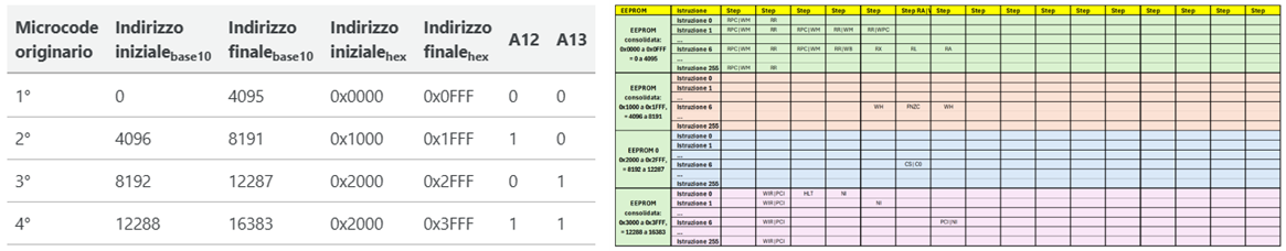
It can be inferred that each EEPROM contains only a portion of the microcode of each instruction, i.e. (obviously) the part relating to the signals wired to its outputs. But how is the microcode distributed across the four EEPROMs? The following table shows, for the example instructions indicated above, which signals are active on each EEPROM during the different steps of the currently executing instruction:

Distribution across the four EEPROMs of the microcode of some example instructions.
Each step of each instruction must therefore be read as the logical concatenation of every nth byte of each EEPROM:
| Instruction | Step | Logical Concatenation |
|---|---|---|
| 0 | 0 | EEPROM0byte0 OR EEPROM1byte0 OR EEPROM2byte0 OR EEPROM3byte0 |
| 0 | 1 | EEPROM0byte1 OR EEPROM1byte1 OR EEPROM2byte1 OR EEPROM3byte1 |
| 0 | … | … |
| 0 | 14 | EEPROM0byte14 OR EEPROM1byte14 OR EEPROM2byte14 OR EEPROM3byte14 |
| 0 | 15 | EEPROM0byte15 OR EEPROM1byte15 OR EEPROM2byte15 OR EEPROM3byte15 |
| 1 | 0 | EEPROM0byte16 OR EEPROM1byte16 OR EEPROM2byte16 OR EEPROM3byte16 |
| 1 | 1 | EEPROM0byte17 OR EEPROM1byte17 OR EEPROM2byte17 OR EEPROM3byte17 |
| 1 | … | … |
| 1 | 14 | EEPROM0byte30 OR EEPROM1byte30 OR EEPROM2byte30 OR EEPROM3byte30 |
| 1 | 15 | EEPROM0byte31 OR EEPROM1byte31 OR EEPROM2byte31 OR EEPROM3byte31 |
For example, the sixth step of the CPX instruction is in fact composed of the concatenation of byte 101 of each EEPROM (instructions and steps are counted starting from zero, therefore (seventh instruction * 16 steps + sixth step) = ((7-1) * 16 + (6-1)) = 96 + 5 = 101):
EEPROM0byte101 + EEPROM1byte101 + EEPROM2byte101 + EEPROM 3byte101, that is
(RL) + (FNZC) + (CS|C0) + (), that is
RL + FNZC + CS|C0, as indicated in the Microcode detail of some example instructions.
In practice, the output signals wired to each EEPROM must be taken into account and it must be indicated which of these should be active at each instruction / step combination. This explains the need to program the four EEPROMs each with its own specific portion of microcode.
Now, rather than performing four separate programming operations, it is much more convenient (albeit more costly) to use four 16KB EEPROMs and write on each of them, in sequence, all four 4KB microcodes initially defined. In this way, four identical 16KB EEPROMs can be programmed, each of which will contain all the 4KB microcode portions.
The table summarizes the placement of the 4KB microcodes consolidated into a single larger EEPROM:
| Original microcode |
Start addressbase10 |
End addressbase10 |
Start addresshex |
End addresshex |
A12 | A13 |
|---|---|---|---|---|---|---|
| 1° | 0 | 4095 | 0x0000 | 0x0FFF | 0 | 0 |
| 2° | 4096 | 8191 | 0x1000 | 0x1FFF | 1 | 0 |
| 3° | 8192 | 12287 | 0x2000 | 0x2FFF | 0 | 1 |
| 4° | 12288 | 16383 | 0x3000 | 0x3FFF | 1 | 1 |
Consolidation of the microcodes into a single EEPROM.
The address columns indicate in which locations of the 16KB EEPROM the individual 4KB instances of the microcode originally defined using four 4KB EEPROMs are placed.

Representation of the four microcodes consolidated into a single EEPROM.
By appropriately setting the addressing lines A12 and A13 of the larger EEPROMs, it is possible to output a specific portion of microcode; see the fixed connections to Vcc or GND in the schematic of the Control Logic. For example, setting A12 to 1 and A13 to 0 will cause a 16KB EEPROM to expose on its outputs the 4KB microcode originally defined for the second 4KB EEPROM.
In other words, we have 256 instructions that develop over 16 steps, each of which consists of a 32-bit Control Word (4 bytes) = 16,384 bytes total. Four 4KB EEPROMs should be programmed: one for the first 8 bits of the Control Word, one for the next 8 bits, and so on. Rather than programming four different 4KB EEPROMs each with a specific portion of microcode, it is possible to program four identical 16KB EEPROMs. In the first 4KB the microcode for the first 8 bits of the Control Word is placed, in the second 4KB the microcode for the next 8 bits, and so on. Finally, the addresses A12 and A13 of the four 16KB EEPROMs are set appropriately, so that each one exposes only the specific portion of microcode relating to the control signals wired to its outputs.
A further visual explanation of what has just been described can be obtained starting from minute 17m:52s of Ben Eater’s video Reprogramming CPU microcode with an Arduino.
Regarding the size count, see also the section Instruction Register (Part 1) and Instructions. One aspect to keep in mind is that 4KB and 16KB parallel EEPROMs are not available on the market, so instead 8KB and 32KB EEPROMs are used by setting the last addressing pin to 0, thus using only the first half of the available space.
With this premise, useful for understanding the distribution of the microcode across the various EEPROMs, we can analyze some important aspects of the Arduino sketch.
Pre-Programming CRC Calculation
Programming the EEPROMs with the original “one byte at a time sequentially” method was, all things considered, fairly straightforward. Much more difficult was proving to be the implementation of Page Write mode, and although I had Tom’s code available to draw from and be inspired by, I kept encountering errors in the microcode stored on the EEPROMs.
Therefore, to determine whether the programmer was working correctly, I had introduced a verification of the correspondence between the Cyclic Redundancy Check (CRC) calculated before writing the microcode and the one calculated by re-reading the EEPROM at the end of its programming cycle.
For simplicity and to facilitate the writing of the code, I imagined a simulated sequential reading of the values to be used to calculate the CRC, starting from address 0x0000 up to address 0x3FFF.
Why simulated? Because at this stage of the program the EEPROM has not yet been programmed, and what is desired at this point is precisely a checksum of the data to be written, a checksum that will then be compared with the one calculated by re-reading the EEPROM at the end of the programming cycle.
We find ourselves in a situation where the CRC calculation routine must receive data sequentially (data that we must produce using the buildInstruction routine responsible for creating instructions and steps); however, buildInstruction performs the splitting of each instruction in the ways described in the previous section, that is, generating a complete opcode and distributing the writes of the 32 bits of the Control Word of each step across the corresponding microcode portions, as highlighted in the table Consolidation of the microcodes into a single EEPROM and in the graphic Representation of the four microcodes consolidated into a single EEPROM.
buildInstruction in fact prepares the 32 bits / 4 bytes of microcode for each step of the current instruction and stores them in a uint32_t array of length 16, i.e. 4 bytes * 16 steps = 64 bytes; subsequently, the writes occur in the following sequence (writeOpcode routine):
- the microcode relating to the first 8 signals* is written to the first 16 bytes of the first portion of the EEPROM (address 0x0000 to 0x000F)
- the microcode relating to the next 8 signals* is written to the first 16 bytes of the second portion of the EEPROM (address 0x1000 to 0x100F)
- the microcode relating to the next 8 signals* is written to the first 16 bytes of the third portion of the EEPROM (address 0x2000 to 0x200F)
- the microcode relating to the last 8 signals* is written to the first 16 bytes of the fourth portion of the EEPROM (address 0x3000 to 0x300F)
The instruction counter is then incremented and the 16 steps of the next instruction are prepared, written taking into account the 16-byte length offset of each instruction:
- the microcode relating to the first 8 signals* is written to the next 16 bytes of the first portion of the EEPROM (address 0x0010 to 0x001F)
- the microcode relating to the next 8 signals* is written to the next 16 bytes of the second portion of the EEPROM (address 0x1010 to 0x101F)
- the microcode relating to the next 8 signals* is written to the next 16 bytes of the third portion of the EEPROM (address 0x2010 to 0x201F)
- the microcode relating to the last 8 signals* is written to the next 16 bytes of the fourth portion of the EEPROM (address 0x3010 to 0x301F)
and so on until the end of the instructions.
* Please refer to the image Definition of the control signals managed by each EEPROM in the previous section.
Returning to the diagram seen previously, buildInstruction prepares instructions and their related steps, for which the writes highlighted by the red arrows (instruction 0) are performed first, followed by those highlighted by the blue arrows (instruction 1), and so on until the last instruction.

Instruction write sequence.
Wanting to reuse the buildInstruction routine, I had to find a way to interpret its output and extract in real time only what I needed in order to achieve that simulated sequential reading discussed at the beginning of this section.
To obtain the desired result, a series of nested loops is executed: for each instruction the 32-bit Control Word of all steps is generated, from which only the 8-bit word relating to the EEPROM portion currently addressed by the outermost loop is extracted.
for (uint8_t rom = 0; rom < 4; rom++)
By doing so, the pre-programming CRC calculation routine sequentially receives as input the 4096 bytes of each of the four microcode portions:
uint16_t calcCRC16_pre(void)
{
  crc = 0xFFFF;
  uint16_t polynomial = 0x1021;
  for (uint8_t rom = 0; rom < 4; rom++)
  {
    for (uint16_t opcode = 0; opcode < 256; opcode++)
    {
      buildInstruction(opcode);
      for (uint8_t step = 0; step < NUM_STEPS; step++)
      {
        // printInstruction(rom, opcode, step); // solo per Debug
        crc = calculate_crc(((code[step]) >> (24 - 8 * rom)) & 0xFF, crc, polynomial);
      }
    }
  }
  return crc;
}
With rom = 0, the crc will be calculated taking into account the 8 most significant bits (right shift of 24 - 8 * 0 = 24 positions) of the 32-bit Control Word generated by buildInstruction and the loop will be executed for all 16 steps of all 256 instructions; when rom = 1, the crc will be calculated taking into account bits 16 to 23 (right shift of 24 - 8 * 1 = 16 positions) of the 32-bit Control Word generated by buildInstruction and the loop will again be executed for all 16 steps of all 256 instructions. The process repeats for rom = 2 and 3, taking into account bits 8 to 15 (right shift of 8 positions) and finally bits 0 to 7 (no right shift).
EEPROM Unlock and Lock
The AT28C256 EEPROMs feature the Software Data Protection function, which prevents unwanted writes: locking and unlocking are performed by sending the EEPROM a short specific sequence of addresses / values according to the specifications on page 10 of the datasheet.
EEPROM Erase
Before programming, the EEPROM is erased. This operation results in greater wear of the EEPROM and lower speed compared to the Software Chip Erase functionality indicated in the Application Note, which has not yet been implemented at this time.
EEPROM Programming
The microcode preparation sequence has already been substantially described in the section Pre-Programming CRC Calculation, since the important microcode generation routine buildInstruction is shared.
The actual programming of the EEPROM, as indicated, follows the fractional logic dictated by my need for code comprehension described earlier (image Instruction write sequence in the section Pre-Programming CRC Calculation), that is, writing one complete opcode at a time. The main routine eeprom_program prepares the opcode via buildInstruction
void eeprom_program()
{
  for (uint16_t opcode = 0; opcode < 256; opcode++)
  {
    buildInstruction((uint8_t) opcode);
    // ...
    writeOpcode((uint8_t) opcode);
  }
  Serial.println("Done!");
}
and calls the writeOpcode routine, which, after every 16 bytes written, in turn calls waitForWriteCycleEnd to verify that the EEPROM is ready to receive new writes, according to the method described in section 4.4 DATA Polling of the datasheet.
void writeOpcode(uint8_t opcode)
{
  for (uint8_t rom = 0; rom < 4; rom++)
  {
    for (uint8_t step = 0; step < NUM_STEPS; step++) // we loop through the 16 steps of each opcode
    // and write them consecutively to each EEPROM portion (Page Write mode)
    {
      uint16_t address;
      address = 0x1000 * rom;
      address += opcode * NUM_STEPS;
      address += step;
      writeEEPROM(address, ((code[step]) >> (24 - 8 * rom)) & 0xFF); // code[step] takes all 4 bytes
      // of the 4 "consolidated" ROMs and then the shift is used to select the byte relating to each
      // specific ROM, for example for the first ROM bits 24-31, then 16-23 etc.
    }
    byte b1Value; // waits for the EEPROM to confirm that it has completed the writes before moving on
    // to the next 16 bytes
    bool status = waitForWriteCycleEnd(((code[15]) >> (24 - 8 * rom)) & 0xFF, &b1Value);
    if (status == false)
    {
      Serial.print("\n******** Error in Opcode 0x");
      Serial.print(opcode, HEX);
      Serial.print(" - Value sent: 0x");
      Serial.print(((code[15]) >> (24 - 8 * rom)) & 0xFF, HEX);
      Serial.print(" - Value read: 0x");
      Serial.println(b1Value, HEX);
      Serial.print("Opcode: 0x");
    }
  }
}
Post-Programming CRC Verification
The post-programming CRC verification is much simpler than the pre-programming one, because in this case there is no need to rely on the buildInstruction routine and work with nested loops to obtain a simulated sequential view of the data: at this point, the EEPROM has actually been programmed and it is sufficient to pass to the CRC calculation routine the values read consecutively from 0x0000 to 0x3FFF.
// POST-PROGRAMMING CRC16 CALCULATION
// When reading a previously programmed EEPROM, all bytes are read sequentially,
// so it is sufficient to read the contents from 0x0000 to 0x3FFF to calculate the checksum.

uint16_t calcCRC16_post(void)
{
  setDataBusMode(INPUT);
  crc = 0xFFFF;
  uint16_t polynomial = 0x1021;
  byte data;
  for (uint16_t address = 0x0000; address <= 0x3FFF; address++)
  {
    data = readEEPROM(address);
    crc = calculate_crc(data, crc, polynomial);
  }
  return crc;
}
At the end, the pre-programming and post-programming CRC values are compared and a positive message is printed in case of a match, along with the total elapsed time.
Notes
In the first section I mentioned that the correct implementation of Page Write mode would require more effort than I had anticipated, but the greatest difficulty was actually encountered in the post-programming CRC verification: the timing of the reads is also critical and I had spent considerable time searching for the correct command sequence. The correct one is the following:
  byte readEEPROM(uint16_t address)
  {
    setAddress(address, true);
    setDataBusMode(INPUT);
    enableChip();
    delayMicroseconds(2);
    byte value = readDataBus();
    disableChip();
    return value;
  }
In my notes I find that the sequence
    setDataBusMode(INPUT);
    enableChip();
    byte value = readDataBus();
caused read errors, whereas by moving enableChip before setDataBusMode, or by adding a 2uS delay, I was able to correctly read the contents of the EEPROM. In the end I had realized that it was preferable to add the 2uS after enabling the chip as the last step, rather than enabling the chip and then setting the data bus to input, because in the following condition a short circuit could have been generated:
- enableChip(): the EEPROM (which has no output resistors) presents one or more LO outputs
- setDataBusMode(INPUT): Arduino presents one or more HI outputs, which are therefore short-circuited to ground by the LO outputs of the EEPROM.
Useful links
-
Ben Eater’s video Using an EEPROM to replace combinational logic, which describes the manual programming of an EEPROM.
-
Ben Eater’s video Build an Arduino EEPROM programmer and the GitHub repository Arduino EEPROM programmer.
-
Tom Nisbet’s TommyProm EEPROM programmer and the simplified sketch needed solely for programming the NQSAP EEPROMs, which I studied to develop the BEAM EEPROM programmer code.