ALU
The 74LS181 - The A register - The NQSAP ALU - The H register - Logic functions and arithmetic operations - Direct (hardwired) relationship between Instruction Register and ALU - Addressing Modes - Comparison instructions - Comparison instructions and Flags - Summary: subtractions, comparisons and addressing modes - Carry, additions and subtractions - Schematic - Differences between NQSAP and BEAM ALU modules - Useful links

The Arithmetic and Logic Unit (ALU) of Ben Eater’s SAP-1 computer was limited to addition and subtraction. Tom Nisbet’s NQSAP added logical and shift operations, and I had started studying it in detail.
The 74LS181
Developed around the 74LS181 chips, the NQSAP ALU had very interesting features but was particularly difficult to understand: it will be one of the modules on which I will spend more time, but which in the end will give the greatest satisfaction for the result.
The ‘181 is a 4-bit ALU developed in the 1970s that can execute 16 arithmetic operations and 16 logic functions. It is possible to chain multiple chips to process wider words.
Use of the terms ‘181 and ALU as equivalents: throughout this page, the terms ALU and ‘181 are often used interchangeably. Note that ALU may refer either to the Arithmetic and Logic Unit module as a whole, or to the ‘181 chip alone. The context will help clarify whether ALU refers to the module or to the chip alone.
Furthermore, since the module uses two ‘181s to compose an 8-bit word, in certain situations the first and second ‘181 — or lower and upper ‘181 — are defined respectively as the one containing the 4 least significant bits (Least Significant Bit, LSB) and the one containing the 4 most significant bits (Most Significant Bit, MSB).
The A register
The A register is not directly connected to the ALU, but, when analyzing at a logical level what happens in the computer, it makes sense to include its description on this page. The A register is a very simple register, similar to the A and B registers already seen in Ben Eater’s SAP-1; the BEAM implements it using a D-type register 74LS377.
The A register of the NQSAP and BEAM differ in construction, but are identical from a functional standpoint. The following schematic, although referring to the BEAM, can be reused in all the explanations that follow, even when primarily aimed at describing the NQSAP ALU module.

The NQSAP ALU
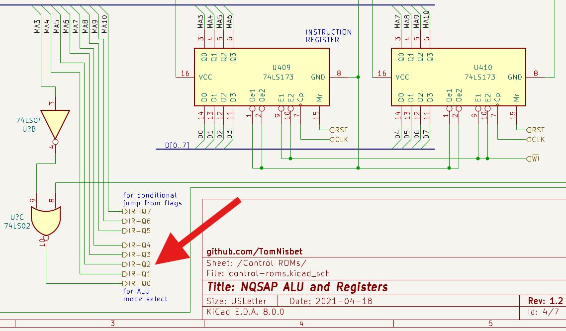
Among the features that stood out in the NQSAP ALU schematic, I noticed above all a large number of chips — among which the 4-bit Bidirectional Universal Shift Register 74LS194 — and a particular way of addressing the ‘181s, which were “tightly coupled” to the instruction present in the Instruction Register of the Control Logic. The relationship with the Control Logic was also among the most complex to analyze and understand, but the one with the Flag module is no less important and its understanding was equally difficult: every ALU operation (and not only) corresponds in fact to an action on the Flag register.

Schematic of Tom Nisbet’s ALU, slightly modified for the sole purpose of improving its readability. The H-Q0 signal is missing, likely a minor omission by Tom.
The ALU module is broadly composed of two input registers H and B and a pair of interconnected ‘181s, which allow an 8-bit word to be handled: H and B are the input registers of the ‘181s.
- The H register is actually a Shift Register capable of both behaving as a normal 8-bit register and shifting the input value left or right.
- The B register is an 8-bit Octal D-Type Flip-Flop with 3-State Outputs 74LS574. The ‘574 does not include an Enable input, which Tom therefore implemented artificially by placing a NOR gate on /Clock and /WB (“Write B”); in this way the register activates only in correspondence with /WB (which is active LO) and the Falling Edge of the inverted clock, equivalent to the Rising Edge of the normal clock, which is the moment when registers are loaded (reference: Ben Eater’s video 8-bit CPU control logic: Part 2). See also the note on glitching in the section The clock and EEPROM “glitching” on the Control Logic page.
- Three ‘245 transceivers allow the values contained in H, B and L to be read (L is the ALU output).
The H register
In Ben Eater’s SAP-1 computer the ALU input registers were A and B, whereas in the NQSAP they are H and B. As mentioned in the previous section, the H register can behave as a common 8-bit register and can replace register A as the ALU input.
Since the 6502 instructions refer to register A, it is necessary that A and H are always aligned, so that the ‘181s transparently find the contents of A in H (for example, an ADC addition will actually be performed by giving the ‘181s registers H and B as input: since H is a copy of A, the result of the addition will be equal to A + B).
What is the usefulness of a “shadow” register like H? Some of the instructions that act directly on a memory location or on a register can be executed without interfering with the contents of register A, for example implicit INX, Absolute Indexed X ASL, and many others.
In all these cases, one of the last steps executed by the microcode will be the copy of A to H:
| ---- | -------------------------- |
| Step | Microinstruction           |
| ---- | -------------------------- |
| 0*   | RPC | WM                   |
| 1*   | RR  | WIR | PCI            |
| 2    | RX  | WH                   |
| 3    | CS  | FNZ | RL | WX        |
| 4    | RA  | WH  | NI             |
| ---- | -------------------------- |
Breakdown of the INX instruction into its five elementary microinstructions.
In the example of the 6502 INX instruction, after the Fetch phase* common to all instructions:
- X is read (RX) and copied into H (WH), which presents its contents to the “A” inputs of the ‘181s;
- the ‘181s perform the A Plus 1 operation, whose result is exposed on the bus (RL) and copied into X (WX);
- A, unmodified, is exposed on the bus (RA) and H is realigned (WH).
Another relevant feature of the H register implemented with ‘194 Shift Registers is the ability to perform shift and rotate operations. The two input pins S0 and S1 define the behavior of the Shift Register on the Rising Edge of the clock:
| S1 | S0 | Operation | ||
|---|---|---|---|---|
| LO | LO | Maintains previous state | ||
| LO | HI | Shifts output bits left (Q3 ← Q2 | Q2 ← Q1 | Q1 ← Q0) and loads Serial Right input into Q0 |
| HI | LO | Shifts output bits right (Q3 → Q2 | Q2 → Q1 | Q1 → Q0) and loads Serial Left input into Q3 |
| HI | HI | Loads inputs P0-P3 into Q0-Q3 |
The schematic shows the execution of a left shift operation, which requires the activation of the control signal HL/S0:

Left shift in the BEAM H register.
At the Rising Edge of the clock the ‘194s shift outputs Q0-Q3 to the left and load into Q0 the values present at the Serial Right (Dsr) inputs, performing all the following operations at the same time:
- the right ‘194 loads into Q0/H0 the H-Cin signal present at its Dsr input, which becomes the new LSB of the shifted byte;
- the left ‘194 loads into Q0/H4 the value of H3 present at its Dsr input;
- the Q0-Q3 outputs of both ‘194s shift to the left.
The 6502 left shift/rotate instructions store the most significant bit of the byte to be shifted in the Carry. The image shows the various 6502 shift and rotate instructions and highlights the left shift.

6502 shift and rotate instructions.
The MSB of H / output H-Q7 highlighted in yellow in the schematic is connected to the Flag module and is saved by the microcode before performing the shift:
| ---- | -------------------------- |
| Step | Microinstruction           |
| ---- | -------------------------- |
| 0*   | RPC | WM                   |
| 1*   | RR  | WIR | PCI            |
| 2    | C1  | FS  | FC             |
| 3    | HL  | CC                   |
| 4    | FNZ | RH  | WA  | NI       |
| ---- | -------------------------- |
Breakdown of the ASL Accumulator instruction into its five elementary microinstructions.
- The first step loads the Program Counter address into the Memory Address Register
- The second step loads the instruction opcode into the IR and increments the PC to make it point to the next memory location (which in the case of the ASL Accumulator instruction contains the next instruction)
- The third step stores the value of H7 in the Carry:
- C1 - selects the Carry source from the MSB (H-Q7) of register H
- FS, Flag Select - Flag source, in this case from another module
- FC, Flag C - updates Flag C
- The fourth step shifts the contents of register H to the left and loads a zero into the LSB
- CC, Carry Clear - presents a value of 0 to the H input
- HL, H Left - performs the shift
- The fifth and final step writes the N and Z Flags and updates A
- RH, Read H - exposes the contents of register H on the bus
- FNZ, Flag N & Z - updates the N and Z Flags computed in the Flag module
- WA, Write A - writes the contents of the bus into A
- NI, Next Instruction - resets the Ring Counter
* The first two steps of all instructions are always the same, as noted in Ring Counter and Microinstructions.
In the schematic the ‘194 is represented with outputs Q0, Q1, Q2 and Q3, which are respectively equivalent to the outputs QA, QB, QC and QD indicated in the datasheet of the ‘194.
Given the flexibility and usefulness of the H Register, this has also been implemented in the BEAM, with a difference in the microcode writing: the NQSAP implements left shift and rotate by exploiting the A Plus A operation of the ‘181s, whereas the BEAM exploits the ‘194s both leftward and rightward.
Logic functions and arithmetic operations
As mentioned in the introduction, the BEAM computer, like the NQSAP, includes the complete 6502 instruction set, including logical and arithmetic instructions. I remembered the main 6502 operations reasonably well and knew well enough what the result of what I was doing should be, but at that point I had no idea yet how it would be possible to achieve it.
In the meantime I had decided to understand the operations made available by the ‘181 and whether there was a logic to their arrangement, a sort of grouping.

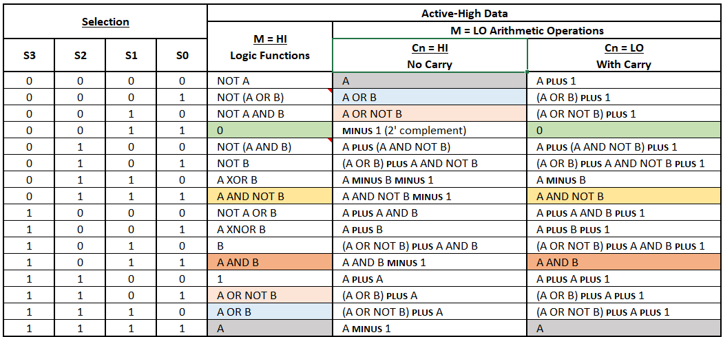
Logic functions and arithmetic operations of the 74LS181.
The ‘181 datasheet was fairly cryptic and so I had also made use of the many resources available online listed at the bottom of the page. From the datasheet it was understood that there are 4 signals S0, S1, S2 and S3 (“Select”) for function/operation selection and a mode control signal M (“Mode”, M = HI for logic functions; M = LO for arithmetic operations); A and B are the data inputs. The datasheet also mentioned Carry Look-Ahead and Ripple-Carry, covered in more depth in one of the sections dedicated to Binary Arithmetic.
Initially I had transcribed the function/operation table into an Excel spreadsheet to be able to work more easily:
Logic functions and arithmetic operations of the 74LS181 - in Excel.
I had highlighted the operations that appeared multiple times, but without finding any grouping or common thread between rows and columns. I was trying to understand the logic behind that seemingly disordered arrangement, but had not found it. Enlightening was Ken Shirriff’s article Inside the vintage 74181 ALU chip: how it works and why it’s so strange.
The most important aspect I had understood is what the two columns of arithmetic operations (performed in correspondence with mode M = LO) had in common:
- without Carry (“Cn = HI –> No Carry”)
- with Carry (“Cn = LO –> With Carry”)
To an experienced eye all of this would have seemed obvious, but I was approaching the topic of the ALU for the first time and many things were not immediately clear to me.
However bizarre some of the available operations may appear (and Ken also explains why), the common thread between the two columns is that the output of the ‘181 is always the same, with the only difference being the absence or presence of the input Carry. Note in fact that, in every row, the output always has a difference of 1, which corresponds to the value of the Carry; for example, in the tenth row we find the simple addition operation A Plus B: the difference between what is computed in the two columns is 1 (A Plus B in case of no input Carry and A Plus B Plus 1 in case of input Carry).
The same reasoning applies to all other available arithmetic operations. Taking the first row as another example: in the absence of Carry, the ALU returns whatever is present at inputs A, whereas in the presence of Carry it adds 1 to whatever is present in A (the arithmetic operation A Plus 1 will later be exploited to create the INC instruction of the computer by “injecting” an artificial Carry into the ‘181; similarly, the DEC instruction was built around the A Minus 1 operation in the table, but in this case without being “boosted” by an artificial Carry).
At this point it is also worth noting that the ‘181 provides two modes of use: one with active-low logic (“Active-Low data”) and one with active-high logic (“Active-High data”) which is the one used in the NQSAP; the latter, to complicate things slightly, expects a negated Carry In input, meaning that a signal Cn (Carry In) = LO is interpreted as an active Carry, while a signal Cn = HI is interpreted as no Carry present. Similarly, the Carry Out is also negated: Cn+4 is in fact HI to indicate that there is no output Carry, while it is LO to indicate that a Carry is present.
Returning to the function/operation table and trying to follow the explanations and logic of the NQSAP, I had understood that the subset visible in this table was sufficient for the intended purpose, which was to be able to emulate the 6502 instructions:
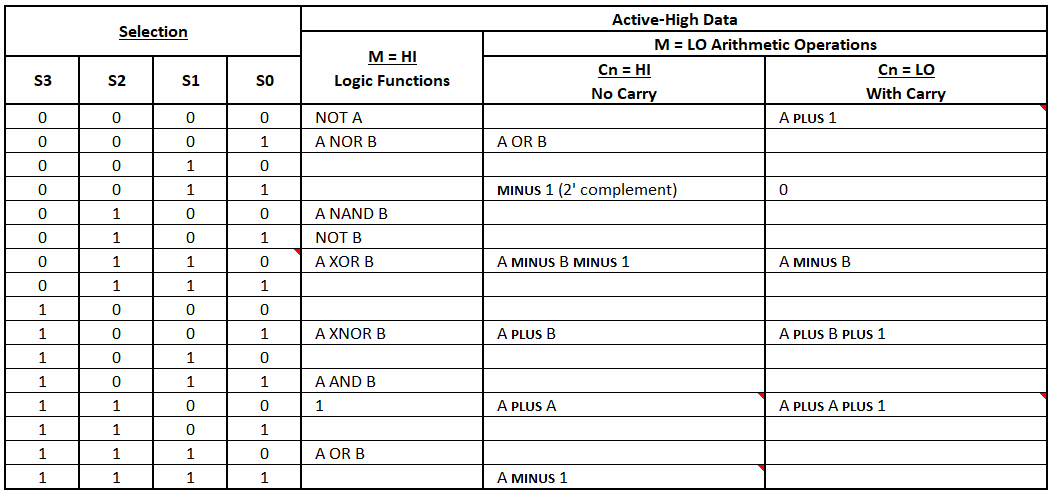
Useful logic and arithmetic operations of the 74LS181.
I would later realize that the required instructions were actually even fewer than I had initially assumed.
Direct (hardwired) relationship between Instruction Register and ALU
Another of the most difficult aspects to understand, as mentioned earlier, was the direct association between the instruction currently contained in the Instruction Register and the logic function / arithmetic operation performed by the ‘181.
Trying to summarize what was drawn in the NQSAP, I had built this table to have an overview of the signals applied to the ALU, their corresponding hexadecimal values and the resulting operations, extrapolating it from the complete instruction table visible in NQSAP Instructions by Address Mode Group, in which the groupings of the NQSAP instructions with respect to the logic functions / arithmetic operations of the ‘181s can be seen quite clearly:
| Cn | M | S3 | S2 | S1 | S0 | Operation | M-S3/S0 Hex |
|---|---|---|---|---|---|---|---|
| 0 | 0 | 0 | 0 | 0 | 1 | A Plus 1 | 0x00 + C* |
| 0 | 0 | 0 | 0 | 1 | 1 | All 0 | 0x03 + C* |
| 0 | 0 | 0 | 1 | 1 | 0 | A Minus B | 0x06 + C* |
| 0 | 0 | 0 | 1 | 1 | 1 | CMP | 0x07** |
| 1 | 0 | 0 | 0 | 1 | 1 | All 1 | 0x03 |
| 1 | 0 | 1 | 0 | 0 | 1 | A Plus B | 0x09 |
| 1 | 0 | 1 | 1 | 0 | 0 | A Plus A | 0x0C*** |
| 1 | 0 | 1 | 1 | 1 | 1 | A Minus 1 | 0x0F |
| x | 1 | 0 | 0 | 0 | 0 | Not A | 0x10**** |
| x | 1 | 0 | 1 | 1 | 0 | A XOR B | 0x16**** |
| x | 1 | 1 | 0 | 1 | 1 | A AND B | 0x1B**** |
| x | 1 | 1 | 1 | 1 | 0 | A OR B | 0x1E**** |
Summary of NQSAP ALU operations.
Legend for the Summary of NQSAP ALU operations table:
-
* I had highlighted these rows as a reminder that on these three operations an artificial Carry had to be “injected” (inverted, therefore the signal actually applied to the Carry In of the first ‘181 had to be LO).
-
** The instructions that modify the state of the 6502 flags are numerous: arithmetic, logical, increment/decrement, rotation, stack, flag, load/transfer register and comparison. The latter (CMP, CPX and CPY) affect only the N, Z and C flags, which are computed by performing a fictitious subtraction (SBC in 6502 terminology) between two values, discarding the result and taking into account only the flags resulting from the subtraction (I had never really looked into how the flags were generated and this exercise was very useful). The operation and differences between subtractions and comparisons are fairly simple to understand:
- in subtractions the value resulting from the subtraction is calculated and retained;
- in comparisons the value resulting from the subtraction is calculated and discarded;
- for both instructions the flags are retained.
To perform comparisons, subtractions are therefore carried out while discarding the result; however, the ‘181 subtraction operations are already used to perform actual subtractions (SBC) and are encoded in the third row of the table with M-S3/S0 = 00110:
Cn M S3 S2 S1 S0 Operation S3/S0 Hex 1 0 0 1 1 0 A Minus B 0x06 + C* How is it possible to perform other subtraction operations using an opcode different from 00110 while knowing that the ‘181s only perform subtractions with this input encoding? We will see this shortly in the section Comparison instructions.
-
*** The A + A operation was used in the NQSAP to shift bits to the left; given the presence of the H Shift Register, I preferred to offload all rotation operations onto it (both right and left, both with and without Carry).
-
**** The Carry is irrelevant as this is a logic function and not an arithmetic operation.
A practical example
It was essentially being said that to perform an addition (“A Plus B”, see sixth row; “ADC” in 6502 terminology) it was necessary to have:
- Cn = 1 (which, as we recall, is managed with inverted logic, so in this case the ALU considers the Carry as not present)
- M = 0
- S3/S2/S1/S0 = 1001
that is:
| Cn | M | S3 | S2 | S1 | S0 | Operation | S3/S0 Hex |
|---|---|---|---|---|---|---|---|
| 1 | 0 | 1 | 0 | 0 | 1 | A Plus B | 0x09 |
In practice, since the M and S3/S0 inputs of the ‘181s are directly connected to the Instruction Register, the addition instruction will necessarily have to be encoded in the microcode by presenting 01001 on the 5 bits shared between the Instruction Register and the ALU
Instruction Register output toward the ALU module with highlight of the 5 selection bits for the ‘181 function / operation.
By activating this instruction, the result exposed at the ‘181s output would have been exactly A Plus B, just as indicated in the tenth row / Cn = HI column of the table extracted from the datasheet “Logic functions and arithmetic operations of the 74LS181”; if we had instead had an input Carry, the exposed result would have been A + B + 1, as indicated in the tenth row / Cn = LO column. The addition (at least in theory) worked and I was also beginning to see in practice the link between the two columns Cn = LO / Cn = HI: the output result was always the same and varied only as a consequence of whether or not there was an input Carry.
The other 3 output bits of the IR were chosen arbitrarily, albeit with some structured considerations, to manage the various addressing modes available on the 6502 that had to be emulated by the NQSAP computer.
Addressing Modes
Each 6502 instruction, such as the aforementioned ADC, offers a certain number of addressing modes among the 13 total available modes (Accumulator, Absolute, Absolute Indexed X or Y, Immediate, Implied, Indirect, Indexed Indirect X, Indirect Indexed Y, Relative, Zero Page, Zero Page Indexed X or Y).
A useful reference for analyzing the relationship between the IR and the ALU was the 6502 Instruction Set page by Norbert Landsteiner, which I also recommend consulting for the 6502 Assembler and the Virtual 6502 that I would later use during microcode debugging.
From the HTML instruction table I had derived an Excel spreadsheet from which I reasoned about the addressing modes, noting that each 6502 instruction never presented more than 8 different addressing modes: hence the other 3 IR output bits allowed a instruction set to be built based on the ‘181 logic functions / arithmetic operations crossed with the (no more than) 8 addressing modes used by each instruction (2^3 = 8 addressable modes usable by each instruction).
The Excel spreadsheet mentioned in the previous paragraph can be downloaded here; the tables just mentioned are present in the “6502 Inst. Set” sheet.
It is also worth noting that, in a computer with only 256 bytes of RAM, Zero Page and Absolute addressing modes are redundant, since both can access the same 256 bytes of memory. Consequently, Zero Page addressing modes (ZP) will not be implemented, as they are equivalent to the Absolute ones.
Returning to the ADC / A Plus B and SBC / A Minus B operations and integrating them with the 3 bits used to manage the addressing modes, one can build — for example — this opcode table:
| Cn | I3 | I2 | I1 | M | S3 | S2 | S1 | S0 | Operaion | Addressing Mode | Hex |
|---|---|---|---|---|---|---|---|---|---|---|---|
| 1 | 0 | 0 | 1 | 0 | 1 | 0 | 0 | 1 | A Plus B | Immediate | 0x29 |
| 1 | 0 | 1 | 0 | 0 | 1 | 0 | 0 | 1 | A Plus B | Absolute | 0x49 |
| 1 | 0 | 1 | 1 | 0 | 1 | 0 | 0 | 1 | A Plus B | Absolute, X | 0x69 |
| 1 | 1 | 0 | 0 | 0 | 1 | 0 | 0 | 1 | A Plus B | Absolute, Y | 0x89 |
| 1 | 1 | 0 | 1 | 0 | 1 | 0 | 0 | 1 | A Plus B | Indexed Indirect X | 0xA9 |
| 1 | 1 | 1 | 0 | 0 | 1 | 0 | 0 | 1 | A Plus B | Indirect Indexed Y | 0xC9 |
| 0 | 0 | 0 | 1 | 0 | 0 | 1 | 1 | 0 | A Minus B | Immediate | 0x26 |
| 0 | 0 | 1 | 0 | 0 | 0 | 1 | 1 | 0 | A Minus B | Absolute | 0x46 |
| 0 | 0 | 1 | 1 | 0 | 0 | 1 | 1 | 0 | A Minus B | Absolute, X | 0x66 |
| 0 | 1 | 0 | 0 | 0 | 0 | 1 | 1 | 0 | A Minus B | Absolute, Y | 0x86 |
| 0 | 1 | 0 | 1 | 0 | 0 | 1 | 1 | 0 | A Minus B | Indexed Indirect X | 0xA6 |
| 0 | 1 | 1 | 0 | 0 | 0 | 1 | 1 | 0 | A Minus B | Indirect Indexed Y | 0xC6 |
Example of the relationship between IR and ALU for all addressing modes of the 6502 ADC and SBC instructions.
It can be noted that the 5 operation bits are always the same for each addressing mode and that only the 3 addressing bits vary depending on the chosen mode.
Starting from this reasoning it became possible to define the opcodes of each instruction to then be encoded in the microcode.
Comparison instructions
We have previously highlighted that the instructions that modify the state of the flags are numerous and that among these are also the comparison instructions.
To explore them further, let us start for example with an instruction that makes use of the flags resulting from a comparison: the conditional jump instruction BMI (Branch on MInus). This instruction is executed only in the presence of the N flag, which indicates that the number resulting from the signed comparison* is Negative, i.e. between -128 and -1 (0x80 and 0xFF in hexadecimal).
* = see the section dedicated to Binary Arithmetic.
As mentioned, the flags of the comparison instructions are calculated by performing a fictitious subtraction between the value contained in register A, X or Y and the value indicated by the operand of the comparison instruction; only the flags resulting from the operation are taken into account and the result of the subtraction is discarded. The flags are therefore generated by exploiting the ‘181 subtraction operation, which is however already used to perform the standard subtraction operation A Minus B (third row of the Summary of NQSAP ALU operations table where M-S3/S2/S1/S0 = 00110 and the microcode will therefore need to present 00110 on the 5 bits shared between the Instruction Register and the ALU).
All the signals that drive the ‘181s derive directly from the Instruction Register (IR), except for the Carry In. It can be said that the ALU is hardwired to the IR and that therefore the computer’s microcode must be written in such a way that the instructions that use the ALU reflect the input signals of the ‘181: for example, observing the previous table Example of the relationship between IR and ALU for all addressing modes of the 6502 ADC and SBC instructions, the A Plus B addition instruction will need to have the bits shared between IR and ALU encoded as 01001, while the A Minus B subtraction instruction will need them encoded as 00110.
| Cn | M | S3 | S2 | S1 | S0 | Operation | M-S3/S0 Hex |
|---|---|---|---|---|---|---|---|
| 0 | 0 | 0 | 1 | 1 | 0 | A Minus B | 0x06 + C* |
| 1 | 0 | 1 | 0 | 0 | 1 | A Plus B | 0x09 |
A very important beneficial side effect of the hardwired connection between IR and ALU is that it is not necessary to dedicate precious ROM outputs for the ‘181 function / operation control lines.
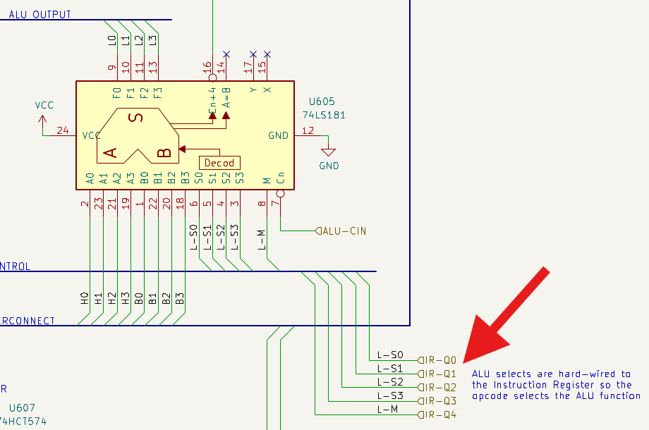
ALU logic function / arithmetic operation selection inputs and “hardwired” connection with the IR.
As can be seen in the excerpt from the schematic Instruction Register output toward the ALU module with highlight of the 5 selection bits for the ‘181 function / operation, the S0 signal is actually only “partially direct” toward the ‘181s, because it first passes through a NOR gate: this is driven by a ROM (pin 8) and activated only in correspondence with comparison instructions, so that the encoding 00111, arbitrarily designated by us to indicate comparison instructions, is presented to the ‘181s as 00110, which is the code for the subtraction instruction (Subtract Mode) and which we need to perform the comparison!
In other words, the microcode of the comparison instructions (which in 6502 mnemonics are CMP, CPX or CPY) will need to activate a signal (“LF”) in one of the EEPROMs: this signal will activate the NOR gate to transmit to the ‘181s the subtraction code 00110 instead of 00111, which originally corresponds to the code for the A And Not B operation, not needed to emulate the 6502 instructions and therefore unused. LF is an abbreviation for ALU Force.
In other words yet:
- The 6502 comparison instructions are executed by simulating a subtraction.
- The subtraction operation is encoded in the ‘181 as M-S3/S0 = 00110 (and cannot be modified).
- How is it possible to handle both actual subtractions and comparisons, considering that both need to present the same encoding 00110 to the ‘181 inputs, which however must be assigned to both subtraction instructions and comparison instructions, which must actually have different opcodes — and therefore different encodings as well?
- An arbitrary opcode is identified for comparison operations by using one that is assigned to an unnecessary operation, for example A And Not B, which has the code M/S3-S0 = 00111.
- The difference between the A Minus B operation and the A And Not B operation lies in the last bit: the former is activated with M-S3/S0 = 00110, the latter with M-S3/S0 = 00111.
- When the IR loads a comparison instruction 00111, it will output that encoding toward the EEPROMs and toward the ALU, but the last bit of that encoding will reach the ALU only after passing through the NOR gate.
- One of the EEPROMs hosting the microcode, when it finds xxx00111 at its input, will activate the LF signal on pin 8 of the NOR gate: the NOR gate will invert the last bit of 00111 and the ‘181s will actually find 00110 at their input, thus configuring themselves in Subtract Mode and performing the subtraction, whose result we will discard in order to retain only the flags.
Comparison instructions and Flags
Initially I had encountered some difficulty in understanding the logic of Flag changes in comparison instructions. Excellent support can be found in a tutorial on 6502.org, which describes how a comparison operation is equivalent to setting the Carry and performing the difference, retaining only the modified Flags and discarding the subtraction result.
If after the comparison operation CMP NUM, which is equivalent to SEC followed by SBC NUM:
- Flag Z is 0, then A <> NUM and the conditional jump BNE is executed
- Flag Z is 1, then A = NUM and the conditional jump BEQ is executed
- Flag C is 0, then A (unsigned) < NUM (unsigned) and the conditional jump BCC is executed
- Flag C is 1, then A (unsigned) >= NUM (unsigned) and the conditional jump BCS is executed
- Flag N is 0, then A (unsigned) >= NUM (unsigned) and the conditional jump BPL is executed
- Flag N is 1, then A (unsigned) < NUM (unsigned) and the conditional jump BMI is executed
After having absorbed the topic, I had some fun with a few tests.
The following code compares the CPY operand with Y and, if Y >= operand, the conditional jump is executed:
LDY #$40
CPY #$30
BCS $60
Before performing the simulated subtraction, the microcode of the CPY instruction sets the Carry; since the value of the operand is less than the value contained in Y, the subtraction does not resort to borrowing the Carry, which at the end of the operation is still set, just as it was at the beginning of the instruction. Finding the Carry active, the subsequent BCS instruction (Branch on Carry Set) is executed.
As above, the following code compares the CPY operand with Y:
LDY #$40
CPY #$40
BNE $60
The comparison activates the Z and C Flags: #$40 - #$40 = 0, therefore the result of the simulated subtraction is equal to zero and Z is set; furthermore, since the number to compare is equal, no borrowing is needed and C remains active. Finding Z active, the subsequent BNE instruction (Branch on Not Equal) is not executed.
The code:
LDY #$40
CPY #$50
BMI $60
activates neither Z nor C, consistently with what was described earlier; it activates N instead, because the simulated subtraction generates a negative result: the MSB takes the value 1, thus activating Flag N. Flag C, set at the beginning of the comparison, takes the value 0 because it is “borrowed”. Finding N active, the subsequent BMI instruction (Branch on MInus) is executed.
Summary: subtractions, comparisons and addressing modes
The NQSAP documentation noted that “since the ALU is tied to the IR, there are only 8 Opcodes available to put it in Subtract Mode”, but I did not understand what this meant. “To create the 16 Opcodes needed for all combinations of Subtract and Compare, a NOR gate is placed on ALU-S0 (IR 0) and on LF, so as to reuse Selection 0111 as if it were 0110, which is Subtract Mode”.
It is important to highlight that the ‘181 Subtract Mode is nothing other than the Input configuration M-S3/S0 = 00110 which corresponds to the arithmetic subtraction operation, as clarified by David Courtney in the video Comparator Functions of 74LS181 (74HCT181) ALU. The datasheet was not so clear regarding the definition of this mode.
The following table highlights how, with 8 bits available for instruction encoding (256 possible combinations), only 8 combinations (2^3, described by bits I2-I1-I0) are the opcodes that allow M and S3/S0 to be in Subtract Mode, i.e. 00110: however, handling all SBC subtraction and CMP, CPX and CPY comparison operations requires far more than 8 combinations, since all combinations of 6502 addressing modes must also be manageable. This is where the LF (ALU Force) signal transforms the encoding 00111 (corresponding to the unused operation A AND NOT B) into 00110, which again activates the ‘181 arithmetic subtraction operation and allows us to obtain 8 + 8 = 16 total opcodes to insert in the microcode for handling subtractions and comparisons in all addressing modes provided in the 6502.
| Bit IR | 7 | 6 | 5 | 4 | 3 | 2 | 1 | 0 |
|---|---|---|---|---|---|---|---|---|
| Signal | I2 | I1 | I0 | M | S3 | S2 | S1 | S0 |
| Opcode | 0 | 0 | 0 | 0 | 0 | 1 | 1 | 0 |
| Opcode | 0 | 0 | 1 | 0 | 0 | 1 | 1 | 0 |
| Opcode | 0 | 1 | 0 | 0 | 0 | 1 | 1 | 0 |
| Opcode | 0 | 1 | 1 | 0 | 0 | 1 | 1 | 0 |
| Opcode | 1 | 0 | 0 | 0 | 0 | 1 | 1 | 0 |
| Opcode | 1 | 0 | 1 | 0 | 0 | 1 | 1 | 0 |
| Opcode | 1 | 1 | 0 | 0 | 0 | 1 | 1 | 0 |
| Opcode | 1 | 1 | 1 | 0 | 0 | 1 | 1 | 0 |
Encoding of the SBC subtraction instruction with the 8 possible addressing combinations determined by the 3 bits I0, I1, I2.
Reading it after having understood it now seems very simple; initially it was anything but.
Carry, additions and subtractions
Some examples will clarify the operation of the Carry using two ‘181s cascaded together to compose an 8-bit word.
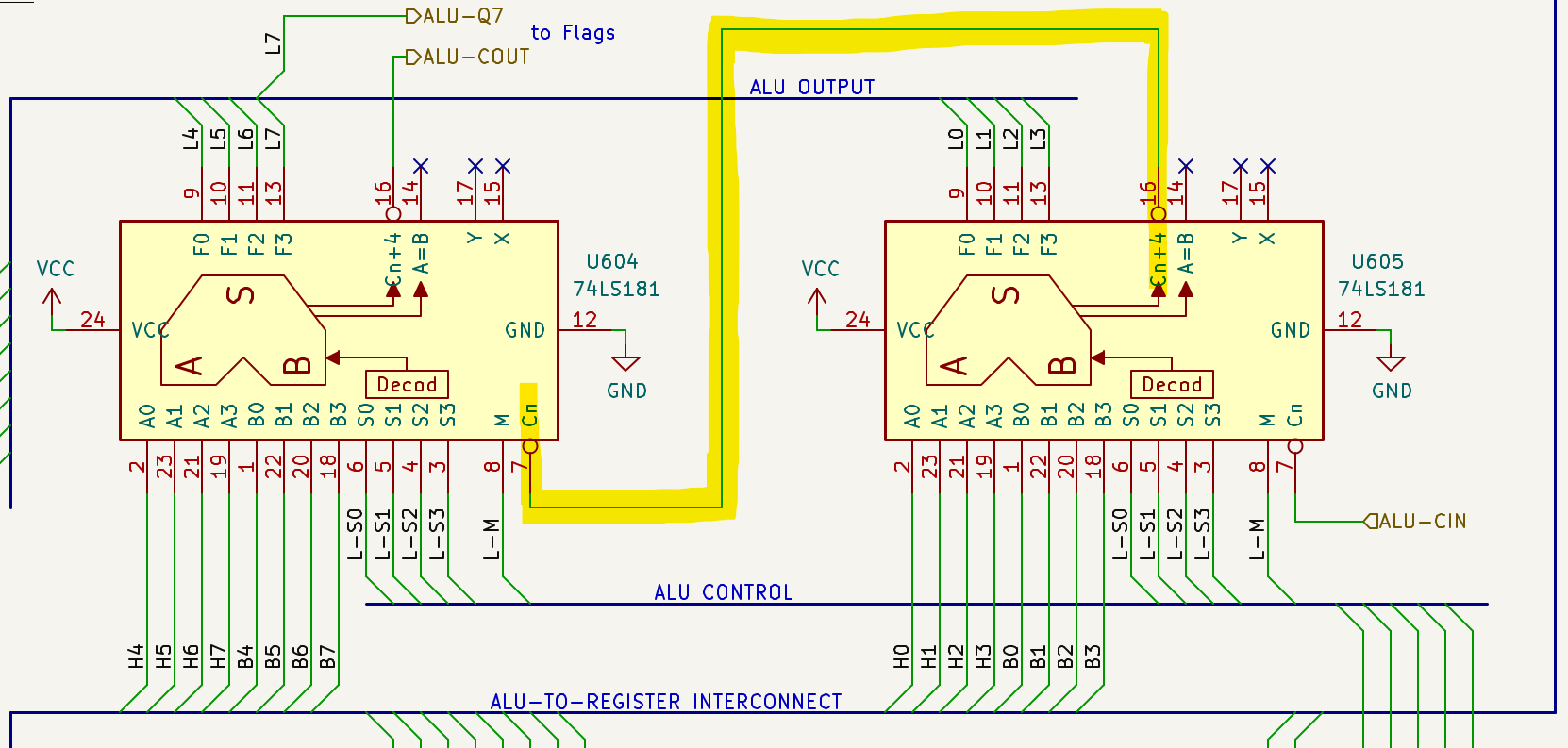
Cascade interconnection of two ‘181 ALUs.
Suppose we perform an A Plus B operation with two ALUs. A signal at logic state HI must be sent to the /Cn input of the first ‘181, which corresponds to having no Carry (recall that in “Active-High Data” logic the Carry is negated). The /Cn+4 (Carry Out) of the first ‘181 enters the /Cn (Carry In) of the second:
-
If the operation performed on the first 4 bits does not generate a carry, the /Cn+4 of the first ‘181 is HI to indicate the absence of Carry; this signal is propagated to the second ‘181, which therefore finds the /Cn input at HI state: both ‘181s perform A Plus B, i.e. a normal operation without carry.
-
Conversely, if the operation performed on the first 4 bits generates a carry, the /Cn+4 of the first ‘181 is LO to indicate the presence of Carry; this signal is propagated to the second ‘181, which therefore finds the /Cn input at LO state: the first ‘181 thus performs the A Plus B operation, while the second performs the A Plus B plus 1 operation: the lower ‘181 essentially generates a carry that is propagated to the upper ‘181.
To perform a subtraction A minus B instead, we must activate the Carry beforehand, i.e. set /Cn = LO.
- If the first ‘181 does not generate a borrow, the /Cn+4 is at logic state LO, which is propagated to the /Cn of the second ‘181 which therefore performs the A Minus B operation.
- If instead the first ‘181 generates a borrow, the /Cn+4 is at logic state HI, which is propagated to the /Cn of the second ‘181 which performs the A Minus B - 1 operation: the lower ‘181 essentially borrows from the upper ‘181.
We can say that the Carry In of the lower ‘181 is used, together with the M-S3/S0 bits, to select the operation that the ALU module will have to perform.
These and other points are explained very well by Tom in the Carry Flag section of his 74181 ALU Notes page dedicated to the ALU.
The use of the Carry in the ‘181 (and consequently in the NQSAP) is similar to what happens in the 6502, with the Carry normally being cleared (CLC) before performing an addition and set (SEC) before performing a subtraction:
- if upon completion of the addition the Carry resulting from the output of the upper ‘181 is set, it means that there is a carry that propagates beyond the 8 bits of the operands;
- conversely, if upon completion of the subtraction the Carry resulting from the output of the upper ‘181 is cleared, it means that a borrow has been requested that propagates beyond the 8 bits of the operands.
The Overflow
From Tom’s very interesting notes I also transcribed that, due to the operating characteristics of the ‘181 and by trying to perform additions or subtractions with and without Carry, one might think of performing a simple exclusive OR (XOR) between the Carry Out (/Cn+4) of the two chips to determine whether the result of the operation generates an Overflow. However the mechanism does not work in the case of A + 1 and A - 1 instructions (and therefore for verifying the existence of Overflow another method will be used, as discussed in the page dedicated to Binary Arithmetic).
Why is the aforementioned check not valid in the case of increment and decrement instructions?
When performing an A + 1 operation (see the signals to be applied to the ‘181 in Summary of NQSAP ALU operations) two cases can occur — let us look at two examples:
- A = 0000.0101 which, incremented by a value of 1, becomes 0000.0110; the increment occurs by injecting a LO signal on the Carry In (/Cn) of the first ‘181; its Carry Out (/Cn+4) is HI, i.e. not active; the result of the operation performed by the second ‘181 does not involve a Carry, therefore its Carry Out (/Cn+4) is still HI.
-
A = 0000.1111 which, incremented by a value of 1, becomes 0001.0000; the increment occurs by injecting a LO signal on the Carry In (/Cn) of the first ‘181; its output Carry (/Cn+4) is LO, i.e. active; the result of the operation performed by the second ‘181 does not involve a Carry, therefore its Carry Out (/Cn+4) is HI.
- In the first case both /Cn+4 are HI and therefore an XOR with inputs connected to those outputs would not signal an Overflow condition, correctly.
- In the second case there is no real Overflow when incrementing the initial word from 0000.1111 to 0001.0000, but if one were to interpret the Carry Outs of the two ‘181s with an XOR function, an error would be made, as the two signals are inverted and the XOR would incorrectly signal Overflow.
All of this is explained very well by Tom on the same page cited a few lines above; as just mentioned, the topic of Overflow is also extensively covered in a dedicated section.
Schematic

Schematic of the BEAM computer ALU.
Differences between NQSAP and BEAM ALU modules
As can be seen from the schematic of the BEAM computer ALU module, this is almost a 1:1 copy of the NQSAP computer ALU module: I certainly did not have the ability to independently develop such a complex ALU module so tightly coupled with other modules of the computer, but the complete understanding of the operation of the ALU developed by Tom nonetheless represented a very important milestone.
Here is a list of the differences:
- For the B register a 74LS377 D-type register was used instead of the 74LS574 used by Tom. Unlike the ‘574, the ‘377 features an Enable input, which only when active allows the register to be loaded on the Rising Edge of the clock: by doing so the need for a gate on the clock input to create an artificial Enable is eliminated, as described in the section The NQSAP ALU.
Schematic of one of the 8 Flip-Flops of the 74LS377.
-
The NQSAP computer provided 8 steps for microinstructions, while the BEAM provides 16. With only 8 steps it would not have been possible to emulate some of the 6502 shift and rotate instructions. This is actually an architectural difference more related to the Control Logic, however the greater number of available steps has an important impact on this module and it therefore certainly makes sense to mention it in this section as well.
-
Tom used the A Plus A operation of the ‘181s to implement the left shift of the 6502 ASL and ROL instructions and the H register for the right shift of the LSR and ROR instructions, while the BEAM uses H in both situations.
Useful links
- Inside the vintage 74181 ALU chip: how it works and why it’s so strange by Ken Shirriff. Essential for understanding the reason behind the apparently so strange implementation of the chip; also excellent is the interactive schematic, which allows the activation of internal signals and outputs to be visualized as a consequence of the applied inputs.
- Tom Nisbet’s notes page on the 74181 ALU Notes.
- Home page of the 74181 on ti.com preserved by Internet Archive.
- Demo of 74LS181 (74HCT181) ALU and Comparator Functions of 74LS181 (74HCT181) ALU: two excellent videos by David Courtney.
- The Micro Logic compendium, from which the image on the 6502 shift and rotate modes is taken.